 搜索
搜索
 发布采购
发布采购
更新日期:2024-04-01 00:04:00

产品简介:具有故障保护功能和 3.3V 至 5V 工作电压的汽车类 RS-485 收发器
查看详情SN65HVD1780QDRQ1 供应商
- 公司
- 型号
- 品牌
- 封装/批号
- 数量
- 地区
- 日期
- 说明
- 询价
-
TI
-
原厂原装
22+ -
3288
-
上海市
-
-
-
一级代理原装
-
TI(德州仪器)
-
SOIC-8
2022+ -
12000
-
上海市
-
-
-
原装可开发票
-
TI
-
SOP
21+ -
5000
-
上海市
-
-
-
原装现货,品质为先!请来电垂询!
SN65HVD1780QDRQ1 中文资料属性参数
- 现有数量:0现货查看交期
- 价格:1 : ¥50.08000剪切带(CT)2,500 : ¥28.36923卷带(TR)
- 系列:Automotive, AEC-Q100
- 包装:卷带(TR)剪切带(CT)? 得捷定制卷带
- 产品状态:在售
- 类型:收发器
- 协议:RS422,RS485
- 驱动器/接收器数:1/1
- 双工:半
- 接收器滞后:50 mV
- 数据速率:115Kbps
- 电压 - 供电:3.15V ~ 5.5V
- 工作温度:-40°C ~ 125°C
- 安装类型:表面贴装型
- 封装/外壳:8-SOIC(0.154",3.90mm 宽)
- 供应商器件封装:8-SOIC
产品特性
- Qualified for Automotive Applications
- AEC-Q100 Qualified With the Following ResultsDevice Temperature Grade 1: –40°C to 125°C Ambient Operating Temperature RangeDevice HBM ESD Classification Level H2Device CDM ESG Classification Level C3B
- Device Temperature Grade 1: –40°C to 125°C Ambient Operating Temperature Range
- Device HBM ESD Classification Level H2
- Device CDM ESG Classification Level C3B
- Bus-Pin Fault Protection to:> ±70 V (’HVD1780-Q1, ’HVD1781-Q1)> ±30 V (’HVD1782-Q1)
- > ±70 V (’HVD1780-Q1, ’HVD1781-Q1)
- > ±30 V (’HVD1782-Q1)
- Operation With 3.3-V to 5-V Supply Range
- ±16-kV HBM Protection on Bus Pins
- Reduced Unit Load for up to 320 Nodes
- Failsafe Receiver for Open-Circuit, Short-Circuit and Idle-Bus Conditions
- Low Power Consumption Low Standby Supply Current, 1 µA Maximum ICC 4-mA Quiescent During Operation
- Low Standby Supply Current, 1 µA Maximum
- ICC 4-mA Quiescent During Operation
- Pin-Compatible With Industry-Standard SN75176
- Signaling Rates of 115 kbps, 1 Mbps, and up to 10 Mbps
产品概述
These devices are designed to survive overvoltage faults such as direct shorts to power
supplies, mis-wiring faults, connector failures, cable crushes, and tool mis-applications. They are
also robust to ESD events, with high levels of protection to the human-body-model
specification. These devices combine a differential driver and a differential receiver, which operate
from a single power supply. In the ’HVD1782, the driver differential outputs and the receiver
differential inputs are connected internally to form a bus port suitable for half-duplex (two-wire
bus) communication. This port features a wide common-mode voltage range, making the devices
suitable for multipoint applications over long cable runs. These devices are characterized from
–40°C to 125°C. These devices are pin-compatible with the industry-standard SN75176 transceiver,
making them drop-in upgrades in most systems. These devices are fully compliant with ANSI TIA/EIA 485-A with a 5-V supply and can
operate with a 3.3-V supply with reduced driver output voltage for low-power applications. For
applications where operation is required over an extended common-mode voltage range, see the
SN65HVD1785 (SLLS872) data sheet.
SN65HVD1780QDRQ1 电路图
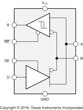
SN65HVD1780QDRQ1 电路图
SN65HVD1780QDRQ1 相关产品
- 14212R-500
- 14222R-800
- 14230R-450
- 14315R-100
- 5962-8771601EA
- 5962-89710013X
- 5962-8971001XX
- 65LBC174AM16DWREP
- 6PAIC3109TRHBRQ1
- 6PAIC3109TWRHMRQ1
- 6PAIC3254IRHBRQ1
- 77049012A
- 7900901CA
- 821004JG
- 821034DNG
- 82V2058XDAG
- 82V2084PFG
- 82V2088BBG
- 88E1510-A0-NNB2C000
- 88E1512-A0-NNP2C000
- 88E1512-A0-NNP2I000
- 88E1514-A0-NNP2C000
- 88E1518-A0-NNB2C000
- 88E3015-A2-NNP1C000
- 88E3082-C1-BAR1C000
- 88E3082-C1-BAR1I000
- 89H64H16AG2ZCBLG
- 89HP0504PBZBNRGI
- 89HPES4T4ZBBCGI
- 89HT0816PYDBCG