 搜索
搜索
 发布采购
发布采购
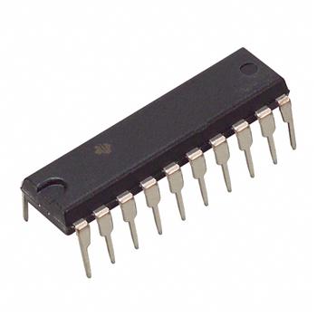
- 封装:20-DIP(0.300",7.62mm)
- RoHS:无铅 / 符合限制有害物质指令(RoHS)规范要求
- 包装方式:管件
- 参考价格:$0.36608-$1
更新日期:2024-04-01 00:04:00
产品简介:具有复位功能的 BiCMOS FCT 接口逻辑八路 D 类触发器
查看详情- 封装:20-DIP(0.300",7.62mm)
- RoHS:无铅 / 符合限制有害物质指令(RoHS)规范要求
- 包装方式:管件
- 参考价格:$0.36608-$1
CD74FCT273E 供应商
- 公司
- 型号
- 品牌
- 封装/批号
- 数量
- 地区
- 日期
- 说明
- 询价
-
TI
-
原厂原装
22+ -
3288
-
上海市
-
-
-
一级代理原装
-
TI(德州仪器)
-
PDIP-20
2022+ -
12000
-
上海市
-
-
-
原装可开发票
CD74FCT273E 中文资料属性参数
- 标准包装:20
- 类别:集成电路 (IC)
- 家庭:逻辑 - 触发器
- 系列:74FCT
- 功能:主复位
- 类型:D 型总线
- 输出类型:非反相
- 元件数:1
- 每个元件的位元数:8
- 频率 - 时钟:70MHz
- 延迟时间 - 传输:7ns
- 触发器类型:正边沿
- 输出电流高,低:15mA,48mA
- 电源电压:4.75 V ~ 5.25 V
- 工作温度:0°C ~ 70°C
- 安装类型:通孔
- 封装/外壳:20-DIP(0.300",7.62mm)
- 包装:管件
- 其它名称:296-33013-5CD74FCT273E-ND
产品特性
- BiCMOS Technology With Low Quiescent Power
- Buffered Inputs
- Direct Clear Input
- 48-mA Output Sink Current
- Output Voltage Swing Limited to 3.7 V
- Controlled Output Edge Rates
- Input/Output Isolation From VCC
- SCR Latch-Up-Resistant BiCMOS Process and Circuit Design
- Applications Include: Buffer/Storage Registers Shift Registers Pattern Generators
- Buffer/Storage Registers
- Shift Registers
- Pattern Generators
- Package Options Include Plastic Small-Outline (M) Package and Standard Plastic (E) DIP
产品概述
The CD74FCT273 is a positive-edge-triggered, D-type flip-flop with a direct clear (CLR\) input. This device uses a small-geometry BiCMOS technology. The output stage is a combination of bipolar and CMOS transistors that limits the output high level to two diode drops below VCC. This resultant lowering of output swing (0 V to 3.7 V) reduces power-bus ringing [a source of electromagnetic interference (EMI)] and minimizes VCC bounce and ground bounce and their effects during simultaneous output switching. The output configuration also enhances switching speed and is capable of sinking 48 mA.
Information at the data (D) inputs meeting the setup time requirements is transferred to the Q outputs on the positive-going edge of the clock (CLK) pulse. Clock triggering occurs at a particular voltage level and is not directly related to the transition time of the positive-going pulse. When CLK is at either the high or low level, the D input has no effect at the output. All eight flip-flops are controlled by a common clock (CLK) and a common reset (CLR\). The outputs are placed in a low state when CLR\ is taken low, independent of the CLK.
The CD74FCT273 is characterized for operation from 0°C to 70°C.
CD74FCT273E 数据手册
| 数据手册 | 说明 | 数量 | 操作 |
|---|---|---|---|
 CD74FCT273E CD74FCT273E
|
IC D-TYPE POS TRG SNGL 20DIP |
12页,507K | 查看 |
CD74FCT273E 相关产品
- 100331QC
- 100351QC
- 74ABT374CSCX
- 74AC11074D
- 74AC11074DR
- 74AC11074N
- 74AC11074PWR
- 74AC16374DLR
- 74AC273MTCX
- 74AC74MTR
- 74AC74SCX
- 74ACT11074D
- 74ACT11074DBR
- 74ACT11074N
- 74ACT11074NSR
- 74ACT11374DWR
- 74ACT16374DLR
- 74ACT16374DLRG4
- 74ACT16823DLR
- 74ACT574SJ
- 74ACT74MTCX
- 74ACT74TTR
- 74AHC1G79GV,125
- 74AHC377PW,118
- 74AHC574PW,118
- 74AHCT273PW,118
- 74AVC16722DGGRE4
- 74F175SCX
- 74F374SCX
- 74HC112PW,118