 搜索
搜索
 发布采购
发布采购
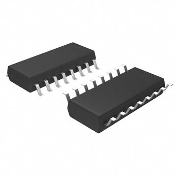
- 封装:16-SOIC(0.209",5.30mm 宽)
- RoHS:无铅 / 符合限制有害物质指令(RoHS)规范要求
- 包装方式:Digi-Reel®
- 参考价格:$0.196-$0.55
更新日期:2024-04-01 00:04:00
产品简介:具有三态输出的 CMOS 四路或非 R/S 锁存器
查看详情- 封装:16-SOIC(0.209",5.30mm 宽)
- RoHS:无铅 / 符合限制有害物质指令(RoHS)规范要求
- 包装方式:Digi-Reel®
- 参考价格:$0.196-$0.55
CD4043BNSR 供应商
- 公司
- 型号
- 品牌
- 封装/批号
- 数量
- 地区
- 日期
- 说明
- 询价
-
TI
-
原厂原装
22+ -
3288
-
上海市
-
-
-
一级代理原装
-
TI(德州仪器)
-
SO-16
2022+ -
12000
-
上海市
-
-
-
原装可开发票
CD4043BNSR 中文资料属性参数
- 标准包装:1
- 类别:集成电路 (IC)
- 家庭:逻辑 - 锁销
- 系列:4000B
- 逻辑类型:S-R 锁存器
- 电路:1:1
- 输出类型:三态
- 电源电压:3 V ~ 18 V
- 独立电路:4
- 延迟时间 - 传输:50ns
- 输出电流高,低:6.8mA,6.8mA
- 工作温度:-55°C ~ 125°C
- 安装类型:表面贴装
- 封装/外壳:16-SOIC(0.209",5.30mm 宽)
- 供应商设备封装:16-SO
- 包装:®
- 其它名称:296-14105-6
产品特性
- 3-state outputs with common output ENABLE
- Separate SET and RESET inputs for each latch
- NOR and NAND configurations
- 5-V, 10-V, and 15-V parametric ratings
- Standardized symmetrical output characteristics
- 100% tested for quiescent current at 20 V
- Maximum input current of 1 µA at 18 V over full package temperature range; 100 nA at 18 V and 25°C
- Noise margin (over full package temperature range): 1 V at VDD = 5 V 2 V at VDD = 10 V 2.5 V at VDD = 15 V
- 1 V at VDD = 5 V
- 2 V at VDD = 10 V
- 2.5 V at VDD = 15 V
- Meets all requirements of JEDEC Tentative Standard No. 13B, "Standard Specifications for Description of 'B' Series CMOS Devices"
- Applications Holding register in multi-register system Four bits of independent storage with output ENABLE Strobed register General digital logic CD4043B for positive logic systems CD4044B for negative logic systems
- Holding register in multi-register system
- Four bits of independent storage with output ENABLE
- Strobed register
- General digital logic
- CD4043B for positive logic systems
- CD4044B for negative logic systems
产品概述
CD4043B types are quad cross-coupled 3-state CMOS NOR latches and the CD4044B types are quad cross-coupled 3-state CMOS NAND latches. Each latch has a separate Q output and individual SET and RESET inputs. The Q outputs are controlled by a common ENABLE input. A logic "1" or high on the ENABLE input connects the latch states to the Q outputs. A logic "0" or low on the ENABLE input disconnects the latch states from the Q outputs, resulting in an open circuit condition on the Q outputs. The open circuit feature allows common busing of the outputs.The CD4043B and CD4044B types are supplied in 16-lead hermetic dual-in-line ceramic packages (F3A suffix), 16-lead dual-in-line plastic packages (E suffix), 16-lead small-outline package (D, DR, DT, DWR, and NSR suffixes), and 16-lead thin shrink small-outline packages (PW and PWR suffixes).
CD4043BNSR 数据手册
| 数据手册 | 说明 | 数量 | 操作 |
|---|---|---|---|
 CD4043BNSR CD4043BNSR
|
CMOS QUAD 3-STATE R/S LATCHES |
13 Pages页,591K | 查看 |
|
CD4043BNSR
|
S-R Latch 4 Channel 1:1 IC Tri-State 16-SO |
31页,1.62M | 查看 |
|
CD4043BNSRG4
|
CMOS Quad NOR R/S Latch with 3-State Outputs 16-SO -55 to 125 |
16页,771K | 查看 |
CD4043BNSR 相关产品
- 74ABT16373ADGGRE4
- 74ABT16373ADGGRG4
- 74ABT373AD,118
- 74ABT573CMTCX
- 74AC16373DLR
- 74AC373PC
- 74ACT11373DBR
- 74ACT11373DWR
- 74ACT16373DLR
- 74ACT16373DLRG4
- 74ACT16841DL
- 74ACT373SCX
- 74ACT841SCX
- 74AHCT573PW,118
- 74ALVC373BQ,115
- 74ALVCH16373DGGRG4
- 74F573SJX
- 74HC259D,652
- 74HC259D,653
- 74HC373D,652
- 74HC573D,652
- 74HC573PW,118
- 74HCT373PW,118
- 74HCT573D,652
- 74LV573PW,118
- 74LVC16373ADGG,118
- 74LVC16373ADGGRG4
- 74LVC16373ADGVRE4
- 74LVC1G373DBVRE4
- 74LVC1G373DCKRE4