 搜索
搜索
 发布采购
发布采购
- 封装:8-SOIC(0.154",3.90mm 宽)
- RoHS:无铅 / 符合限制有害物质指令(RoHS)规范要求
- 包装方式:管件
- 参考价格:$10.005-$9.177
更新日期:2024-04-01 00:04:00
产品简介:高增益可调范围、宽带压控放大器
查看详情- 封装:8-SOIC(0.154",3.90mm 宽)
- RoHS:无铅 / 符合限制有害物质指令(RoHS)规范要求
- 包装方式:管件
- 参考价格:$10.005-$9.177
VCA810ID 供应商
- 公司
- 型号
- 品牌
- 封装/批号
- 数量
- 地区
- 日期
- 说明
- 询价
-
TI
-
原厂原装
22+ -
3288
-
上海市
-
-
-
一级代理原装
-
BB
-
SOIC-8
10+ -
124
-
杭州
-
-
-
原装正品现货
-
BB
-
-
2019+ -
5800
-
上海市
-
-
-
全新原装现货
-
TI(德州仪器)
-
SOIC-8
2022+ -
12000
-
上海市
-
-
-
原装可开发票
-
BB
-
SMD
23+ -
15000
-
上海市
-
-
-
中国区代理原装进口特价
-
BB
-
100/T
21+ -
2000
-
上海市
-
-
-
原装现货,品质为先,请来电垂询!
-
BB
-
SMD
22+ -
5728
-
常州
-
-
-
全新原装现货热卖
-
TI
-
SOIC8
23+ -
5800
-
上海市
-
-
-
进口原装现货,杜绝假货。
-
TI/德州仪器
-
SOP8
21+ -
10000
-
杭州
-
-
-
只做原装现货,大量现货热卖
VCA810ID 中文资料属性参数
- 标准包装:75
- 类别:集成电路 (IC)
- 家庭:Linear - Amplifiers - Instrumentation, OP Amps, Buffer Amps
- 系列:-
- 放大器类型:可变增益
- 电路数:1
- 输出类型:-
- 转换速率:350 V/µs
- 增益带宽积:-
- -3db带宽:35MHz
- 电流 - 输入偏压:6µA
- 电压 - 输入偏移:100µV
- 电流 - 电源:20mA
- 电流 - 输出 / 通道:60mA
- 电压 - 电源,单路/双路(±):±4 V ~ 6 V
- 工作温度:-40°C ~ 85°C
- 安装类型:表面贴装
- 封装/外壳:8-SOIC(0.154",3.90mm 宽)
- 供应商设备封装:8-SOIC
- 包装:管件
- 配用:296-19684-ND - BOARD DEMO FOR 8SOIC VCA'S
- 其它名称:296-17317296-17317-5296-17317-ND
产品特性
- High Gain Adjust Range: ±40 dB
- Differential In, Single-Ended Out
- Low Input Noise Voltage: 2.4 nV/√Hz
- Constant Bandwidth vs Gain: 35 MHz
- High dB/V Gain Linearity: ±0.3 dB
- Gain Control Bandwidth: 25 MHz
- Low Output DC Error: < ±40 mV
- High Output Current: &plsumn;60 mA
- Low Supply Current: 24.8 mA (Maximum for –40°C to 85°C Temperature Range)
- APPLICATIONS Optical Receiver Time Gain Control Sonar Systems Voltage-Tunable Active Filters Log Amplifiers Pulse Amplitude Compensation AGC receivers With RSSI Improved Replacement for VCA610
- Optical Receiver Time Gain Control
- Sonar Systems
- Voltage-Tunable Active Filters
- Log Amplifiers
- Pulse Amplitude Compensation
- AGC receivers With RSSI
- Improved Replacement for VCA610
产品概述
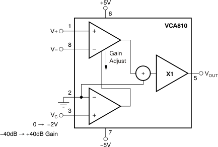
The VCA810 is a DC-coupled, wideband, continuously variable, voltage-controlled gain
amplifier. The device provides a differential input to single-ended output conversion with a
high-impedance gain control input used to vary the gain over a –40-dB to 40-dB range linear in
dB/V.Operating from ±5-V supplies, the device gain control voltage adjusts the gain from –40
dB at a 0-V input to 40 dB at a –2-V input. Increasing the control voltage above ground attenuates
the signal path to greater than 80 dB. Signal bandwidth and slew rate remain constant over the
entire gain adjust range. This 40-dB/V gain control is accurate within ±1.5 dB (±0.9 dB for high
grade), allowing the gain control voltage in an AGC application to be used as a received signal
strength indicator (RSSI) with ±1.5-dB accuracy.Excellent common-mode rejection and common-mode input range at the two high-impedance
inputs allow the device to provide a differential receiver operation with gain adjust. The output
signal is referenced to ground. Zero differential input voltage gives a 0-V output with a small DC
offset error. Low input noise voltage ensures good output SNR at the highest gain settings.In applications where pulse edge information is critical, and the device is being used to
equalize varying channel loss, minimal change in group delay over gain setting retains excellent
pulse edge information.An improved output stage provides adequate output current to drive the most demanding
loads. Although principally intended to drive analog-to-digital converters (ADCs) or second-stage
amplifiers, the ±60-mA output current easily drives doubly-terminated 50-Ω lines or a passive
post-filter stage over the ±1.7-V output voltage range.
VCA810ID 数据手册
 VCA810ID
VCA810ID 电路图
VCA810ID 电路图
VCA810ID 相关产品
- ACPL-7900-000E
- ACPL-7900-300E
- ACPL-790A-000E
- ACPL-790B-000E
- ACPL-790B-300E
- ACPL-C784-000E
- ACPL-C790-500E
- ACPL-C79A-500E
- ACPL-C79B-500E
- AD202JY
- AD202KN
- AD202KY
- AD210AN
- AD210BN
- AD521JDZ
- AD521KDZ
- AD521LDZ
- AD524AE
- AD524ARZ-16-REEL7
- AD524BE
- AD524CD
- AD526BDZ
- AD526CD
- AD526CDZ
- AD526JNZ
- AD526SD
- AD548JRZ-REEL
- AD548KNZ
- AD5748ACPZ-RL7
- AD5749ACPZ-RL7