
 搜索
搜索
 发布采购
发布采购
- RoHS:
• 镉(Cd)/镉化合物 0.01%
• 六价隔(Cr6+)/六价隔化合物 0.10%
• 铅(Pb)/铅化合物 0.10%
• 汞(Hg)/汞化合物 0.10%
• 多溴联苯(PBB)0.10%
• 多溴联苯醚(PBDE)0.10% - 含十溴二苯醚(Deca-BDE) 0.10%
说明:Translation - Voltage Levels EP 8B Dual-Sply Bus Xcvr - 参考价格:¥10.70-¥9.52
更新日期:2024-04-01 00:04:00

产品简介:具有可配置电压转换和三态输出的 8 位双电源总线收发器(增强型产品)
查看详情- RoHS:
• 镉(Cd)/镉化合物 0.01%
• 六价隔(Cr6+)/六价隔化合物 0.10%
• 铅(Pb)/铅化合物 0.10%
• 汞(Hg)/汞化合物 0.10%
• 多溴联苯(PBB)0.10%
• 多溴联苯醚(PBDE)0.10% - 含十溴二苯醚(Deca-BDE) 0.10%
说明:Translation - Voltage Levels EP 8B Dual-Sply Bus Xcvr - 参考价格:¥10.70-¥9.52
V62/09615-01XE 中文资料属性参数
- 制造商:Texas Instruments
- 产品种类:转换 - 电压电平
- 传播延迟时间:28.8 ns
- Supply Voltage - Max:5.5 V
- Supply Voltage - Min:1.65 V
- 最大工作温度:+ 125 C
- 安装风格:SMD/SMT
- 封装 / 箱体:TSSOP-24
- 最小工作温度:- 55 C
- 输出类型:3-State
- 封装:Reel
- 工厂包装数量:2000
产品特性
- Control Inputs VIH/VIL Levels Are Referenced to VCCA Voltage
- VCC Isolation Feature – If Either VCC Input Is at GND, All Are in the High-Impedance State
- Fully Configurable Dual-Rail Design Allows Each Port to Operate Over the Full 1.65-V to 5.5-V Power-Supply Range
- Latch-Up Performance Exceeds 100 mA Per JESD 78, Class II
- ESD Protection Exceeds JESD 22 4000-V Human-Body Model (A114-A) 200-V Machine Model (A115-A) 1000-V Charged-Device Model (C101)
- 4000-V Human-Body Model (A114-A)
- 200-V Machine Model (A115-A)
- 1000-V Charged-Device Model (C101)
产品概述
This 8-bit noninverting bus transceiver uses two separate configurable power-supply
rails. The SN74LVC8T245-EP is optimized to operate with VCCA and
VCCB set at 1.65 V to 5.5 V. The A port is designed to track
VCCA. VCCA accepts any supply voltage from 1.65 V to
5.5 V. The B port is designed to track VCCB. VCCB
accepts any supply voltage from 1.65 V to 5.5 V. This allows for universal low-voltage
bidirectional translation between any of the 1.8-V, 2.5-V, 3.3-V, and 5.5-V voltage nodes.The SN74LVC8T245-EP is designed for asynchronous communication between two data buses.
The logic levels of the direction-control (DIR) input and the output-enable
(OE) input activate either the B-port outputs or the A-port outputs or place
both output ports into the high-impedance mode. The device transmits data from the A bus to the B
bus when the B-port outputs are activated, and from the B bus to the A bus when the A-port outputs
are activated. The input circuitry on both A and B ports is always active and must have a logic
HIGH or LOW level applied to prevent excess ICC and
ICCZ.The SN74LVC8T245-EP is designed so that the control pins (DIR and
OE) are supplied by VCCA.This device is fully specified for partial-power-down applications using
Ioff. The Ioff circuitry disables the outputs,
preventing damaging current backflow through the device when it is powered down.The VCC isolation feature ensures that if either
VCC input is at GND, all outputs are in the high-impedance state.To ensure the high-impedance state during power up or power down,
OE should be tied to VCC through a pullup resistor;
the minimum value of the resistor is determined by the current-sinking capability of the
driver.
V62/09615-01XE 电路图
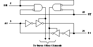
V62/09615-01XE 电路图
V62/09615-01XE 相关产品
- 100301QC
- 100304QC
- 100310QC
- 100311QC
- 100313QC
- 100316QC
- 100322QC
- 100329APC
- 100329DC
- 100336DC
- 100336PC
- 100341QC
- 100351DC
- 100351PC
- 100363QC
- 100364QC
- 100370QC
- 100390QC
- 100398QI
- 11AA010T-I/TT
- 11AA160T-I/TT
- 11LC010T-I/TT
- 11LC020T-I/TT
- 11LC040T-E/TT
- 11LC160T-E/TT
- 1ED020I12-F
- 2304NZGI-1LF
- 23A640-I/SN
- 23K256-I/SN
- 23K256-I/ST