 搜索
搜索
 发布采购
发布采购
- RoHS:
• 镉(Cd)/镉化合物 0.01%
• 六价隔(Cr6+)/六价隔化合物 0.10%
• 铅(Pb)/铅化合物 0.10%
• 汞(Hg)/汞化合物 0.10%
• 多溴联苯(PBB)0.10%
• 多溴联苯醚(PBDE)0.10% - 含十溴二苯醚(Deca-BDE) 0.10%
说明:Latches Mil Enh 16B Transp D-Type Latch - 参考价格:¥19.11-¥22.77
更新日期:2024-04-01 00:04:00
产品简介:具有三态输出的 16 位 D 级透明锁存器(增强型产品)
查看详情- RoHS:
• 镉(Cd)/镉化合物 0.01%
• 六价隔(Cr6+)/六价隔化合物 0.10%
• 铅(Pb)/铅化合物 0.10%
• 汞(Hg)/汞化合物 0.10%
• 多溴联苯(PBB)0.10%
• 多溴联苯醚(PBDE)0.10% - 含十溴二苯醚(Deca-BDE) 0.10%
说明:Latches Mil Enh 16B Transp D-Type Latch - 参考价格:¥19.11-¥22.77
V62/06649-01XE 中文资料属性参数
- 制造商:Texas Instruments
- 产品种类:闭锁
- 电路数量:2
- 逻辑类型:D-Type Transparent Latch
- 逻辑系列:LVC
- 极性:Non-Inverting
- 输出线路数量:16
- 高电平输出电流:- 24 mA
- 低电平输出电流:32 mA
- 传播延迟时间:5.2 ns at 2.5 V, 4.9 ns at 2.7 V, 4.2 ns at 3.3 V
- Supply Voltage - Max:3.6 V
- Supply Voltage - Min:1.65 V
- 最大工作温度:+ 125 C
- 最小工作温度:- 55 C
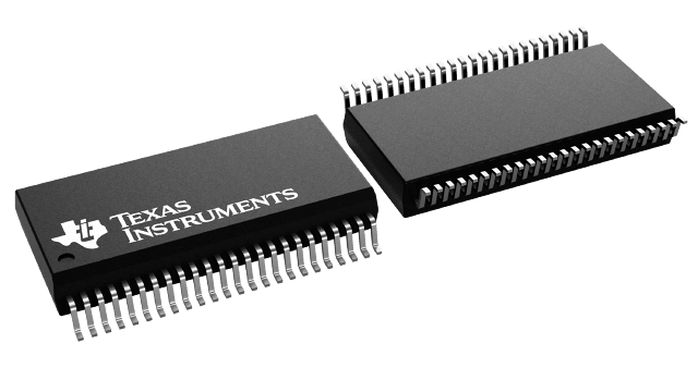
- 封装 / 箱体:SSOP-48
- 封装:Reel
- 安装风格:SMD/SMT
- 输入线路数量:16
- 工厂包装数量:1000
产品特性
- Member of the Texas Instruments Widebus™ Family
- Operates From 1.65 V to 3.6 V
- Inputs Accept Voltages to 5.5 V
- Max tpd of 4.2 ns at 3.3 V
- Typical VOLP (Output Ground Bounce) <0.8 V at VCC = 3.3 V, TA = 25°C
- Typical VOHV (Output VOH Undershoot) >2 V at VCC = 3.3 V, TA = 25°C
- Ioff Supports Partial-Power-Down Mode Operation
- Supports Mixed-Mode Signal Operation (5-V Input and Output Voltages With 3.3-V VCC)
- Latch-Up Performance Exceeds 100 mA Per JESD 78, Class II
- ESD Protection Exceeds JESD 22 2000-V Human-Body Model (A114-A)1000-V Charged-Device Model (C101)
- 2000-V Human-Body Model (A114-A)
- 1000-V Charged-Device Model (C101)
产品概述
This 16-bit transparent D-type latch is designed for 1.65-V to 3.6-V VCC operation.The SN74LVC16373A is particularly suitable for implementing buffer registers, I/O ports, bidirectional bus drivers, and working registers. The device can be used as two 8-bit latches or one 16-bit latch. When the latch-enable (LE) input is high, the Q outputs follow the data (D) inputs. When LE is taken low, the Q outputs are latched at the levels set up at the D inputs.A buffered output-enable (OE) input can be used to place the eight outputs in either a normal logic state (high or low logic levels) or the high-impedance state. In the high-impedance state, the outputs neither load nor drive the bus lines significantly. The high-impedance state and increased drive provide the capability to drive bus lines without interface or pullup components.OE does not affect internal operations of the latch. Old data can be retained or new data can be entered while the outputs are in the high-impedance state.Inputs can be driven from either 3.3-V or 5-V devices. This feature allows the use of this device as a translator in a mixed 3.3-V/5-V system environment.To ensure the high-impedance state during power up or power down, OE should be tied to VCC through a pullup resistor; the minimum value of the resistor is determined by the current-sinking capability of the driver.This device is fully specified for partial-power-down applications using Ioff. The Ioff circuitry disables the outputs, preventing damaging current backflow through the device when it is powered down.
V62/06649-01XE 相关产品
- 100301QC
- 100304QC
- 100310QC
- 100311QC
- 100313QC
- 100316QC
- 100322QC
- 100329APC
- 100329DC
- 100336DC
- 100336PC
- 100341QC
- 100351DC
- 100351PC
- 100363QC
- 100364QC
- 100370QC
- 100390QC
- 100398QI
- 11AA010T-I/TT
- 11AA160T-I/TT
- 11LC010T-I/TT
- 11LC020T-I/TT
- 11LC040T-E/TT
- 11LC160T-E/TT
- 1ED020I12-F
- 2304NZGI-1LF
- 23A640-I/SN
- 23K256-I/SN
- 23K256-I/ST