 搜索
搜索
 发布采购
发布采购
- RoHS:
• 镉(Cd)/镉化合物 0.01%
• 六价隔(Cr6+)/六价隔化合物 0.10%
• 铅(Pb)/铅化合物 0.10%
• 汞(Hg)/汞化合物 0.10%
• 多溴联苯(PBB)0.10%
• 多溴联苯醚(PBDE)0.10% - 含十溴二苯醚(Deca-BDE) 0.10%
说明:Flip Flops Mil Enh Sgl Pos Edge-Trgrd D-Type - 参考价格:¥1.95-¥2.28
更新日期:2024-04-01
产品简介:增强型产品单路上升沿 D 类触发器
查看详情- RoHS:
• 镉(Cd)/镉化合物 0.01%
• 六价隔(Cr6+)/六价隔化合物 0.10%
• 铅(Pb)/铅化合物 0.10%
• 汞(Hg)/汞化合物 0.10%
• 多溴联苯(PBB)0.10%
• 多溴联苯醚(PBDE)0.10% - 含十溴二苯醚(Deca-BDE) 0.10%
说明:Flip Flops Mil Enh Sgl Pos Edge-Trgrd D-Type - 参考价格:¥1.95-¥2.28
V62/05621-01XE 中文资料属性参数
- 制造商:Texas Instruments
- 产品种类:触发器
- 电路数量:1
- 逻辑系列:LVC
- 逻辑类型:CMOS
- 极性:Non-Inverting
- 输入类型:Single-Ended
- 输出类型:Single-Ended
- 传播延迟时间:5 ns
- 高电平输出电流:- 32 mA
- 低电平输出电流:32 mA
- Supply Voltage - Max:5.5 V
- 最大工作温度:+ 115 C
- 安装风格:SMD/SMT
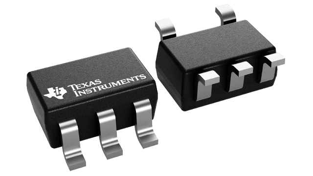
- 封装 / 箱体:SC-70
- 封装:Reel
- 最小工作温度:- 55 C
- 输入线路数量:1
- 输出线路数量:1
- 工厂包装数量:3000
- Supply Voltage - Min:1.65 V
产品特性
- Supports 5-V VCC Operation
- Inputs Accept Voltages to 5.5 V
- Max tpd of 5 ns at 3.3 V
- Low Power Consumption, 10-µA Max ICC
- ±24-mA Output Drive at 3.3 V
- Ioff Supports Partial-Power-Down Mode Operation
- Latch-Up Performance Exceeds 100 mA Per JESD 78, Class II
- ESD Protection Exceeds JESD 22 2000-V Human-Body Model (A114-A) 200-V Machine Model (A115-A) 1000-V Charged-Device Model (C101)
- 2000-V Human-Body Model (A114-A)
- 200-V Machine Model (A115-A)
- 1000-V Charged-Device Model (C101)
- SUPPORTS DEFENSE, AEROSPACE, AND MEDICAL APPLICATIONS Controlled Baseline One Assembly/Test Site One Fabrication Site Available in Military (–55°C/125°C) Temperature Range(1) Extended Product Life Cycle Extended Product-Change Notification Product Traceability
- Controlled Baseline
- One Assembly/Test Site
- One Fabrication Site
- Available in Military (–55°C/125°C) Temperature Range(1)
- Extended Product Life Cycle
- Extended Product-Change Notification
- Product Traceability
产品概述
This single positive-edge-triggered D-type flip-flop is designed for 1.65-V to 5.5-V VCC operation.When data at the data (D) input meets the setup time requirement, the data is transferred to the Q output on the positive-going edge of the clock pulse. Clock triggering occurs at a voltage level and is not directly related to the rise time of the clock pulse. Following the hold-time interval, data at the D input can be changed without affecting the level at the output.This device is fully specified for partial-power-down applications using Ioff. The Ioff circuitry disables the outputs, preventing damaging current backflow through the device when it is powered down.
V62/05621-01XE 相关产品
- 100301QC
- 100304QC
- 100310QC
- 100311QC
- 100313QC
- 100316QC
- 100322QC
- 100329APC
- 100329DC
- 100336DC
- 100336PC
- 100341QC
- 100351DC
- 100351PC
- 100363QC
- 100364QC
- 100370QC
- 100390QC
- 100398QI
- 11AA010T-I/TT
- 11AA160T-I/TT
- 11LC010T-I/TT
- 11LC020T-I/TT
- 11LC040T-E/TT
- 11LC160T-E/TT
- 1ED020I12-F
- 2304NZGI-1LF
- 23A640-I/SN
- 23K256-I/SN
- 23K256-I/ST