 搜索
搜索
 发布采购
发布采购
- RoHS:
• 镉(Cd)/镉化合物 0.01%
• 六价隔(Cr6+)/六价隔化合物 0.10%
• 铅(Pb)/铅化合物 0.10%
• 汞(Hg)/汞化合物 0.10%
• 多溴联苯(PBB)0.10%
• 多溴联苯醚(PBDE)0.10% - 含十溴二苯醚(Deca-BDE) 0.10%
说明:Universal Bus Functions Mil Enh 8B Uni Bus & Two 1B Bus Xcvrs - 参考价格:¥22.84-¥23.87
更新日期:2024-04-01 00:04:00
产品简介:增强型产品,8 位通用总线收发器和 2 个 1 位总线收发器
查看详情- RoHS:
• 镉(Cd)/镉化合物 0.01%
• 六价隔(Cr6+)/六价隔化合物 0.10%
• 铅(Pb)/铅化合物 0.10%
• 汞(Hg)/汞化合物 0.10%
• 多溴联苯(PBB)0.10%
• 多溴联苯醚(PBDE)0.10% - 含十溴二苯醚(Deca-BDE) 0.10%
说明:Universal Bus Functions Mil Enh 8B Uni Bus & Two 1B Bus Xcvrs - 参考价格:¥22.84-¥23.87
V62/05606-01YE 中文资料属性参数
- 制造商:Texas Instruments
- 产品种类:通用总线函数
- 逻辑类型:CMOS
- 逻辑系列:VME
- 电路数量:1
- 传播延迟时间:10.5 ns
- Supply Voltage - Max:3.45 V
- Supply Voltage - Min:3.15 V
- 最大工作温度:+ 85 C
- 最小工作温度:- 40 C
- 封装 / 箱体:TVSOP
- 封装:Reel
- 功能:Universal Bus Transceiver
- 高电平输出电流:- 48 mA
- 低电平输出电流:64 mA
- 安装风格:SMD/SMT
- 工作电源电压:3.3 V
- 输出类型:3-State
- 极性:Non-Inverting
- 工厂包装数量:2000
产品特性
- Controlled BaselineOne Assembly/Test Site, One Fabrication Site
- One Assembly/Test Site, One Fabrication Site
- Enhanced Diminishing Manufacturing Sources (DMS) Support
- Enhanced Product-Change Notification
- Qualification Pedigree(1)
- Member of the Texas Instruments Widebus Family
- UBT Transceiver Combines D-Type Latches and D-Type Flip-Flops for Operation in Transparent, Latched, or Clocked Modes
- OEC Circuitry Improves Signal Integrity and Reduces Electromagnetic Interference (EMI)
- Compliant With VME64, 2eVME, and 2eSST Protocols Validated at TA = -40°C to 85°C
- Bus Transceiver Split LVTTL Port Provides a Feedback Path for Control and Diagnostics Monitoring
- I/O Interfaces are 5-V Tolerant
- B-Port Outputs (-48 mA/64 mA)
- Y and A-Port Outputs (-12 mA/12 mA)
- Ioff, Power-Up 3-State, and BIAS VCC Support Live Insertion
- Bus Hold on 3A-Port Data Inputs
- 26-Ω Equivalent Series Resistor on 3A Ports and Y Outputs
- Flow-Through Architecture Facilitates Printed Circuit Board Layout
- Distributed VCC and GND Pins Minimize High-Speed Switching Noise
- Latch-Up Performance Exceeds 100 mA Per JESD 78, Class II
- ESD Protection Exceeds JESD 222000-V Human-Body Model (A114-A) 200-V Machine Model (A115-A) 1000-V Charged-Device Model (C101)
- 2000-V Human-Body Model (A114-A)
- 200-V Machine Model (A115-A)
- 1000-V Charged-Device Model (C101)
产品概述
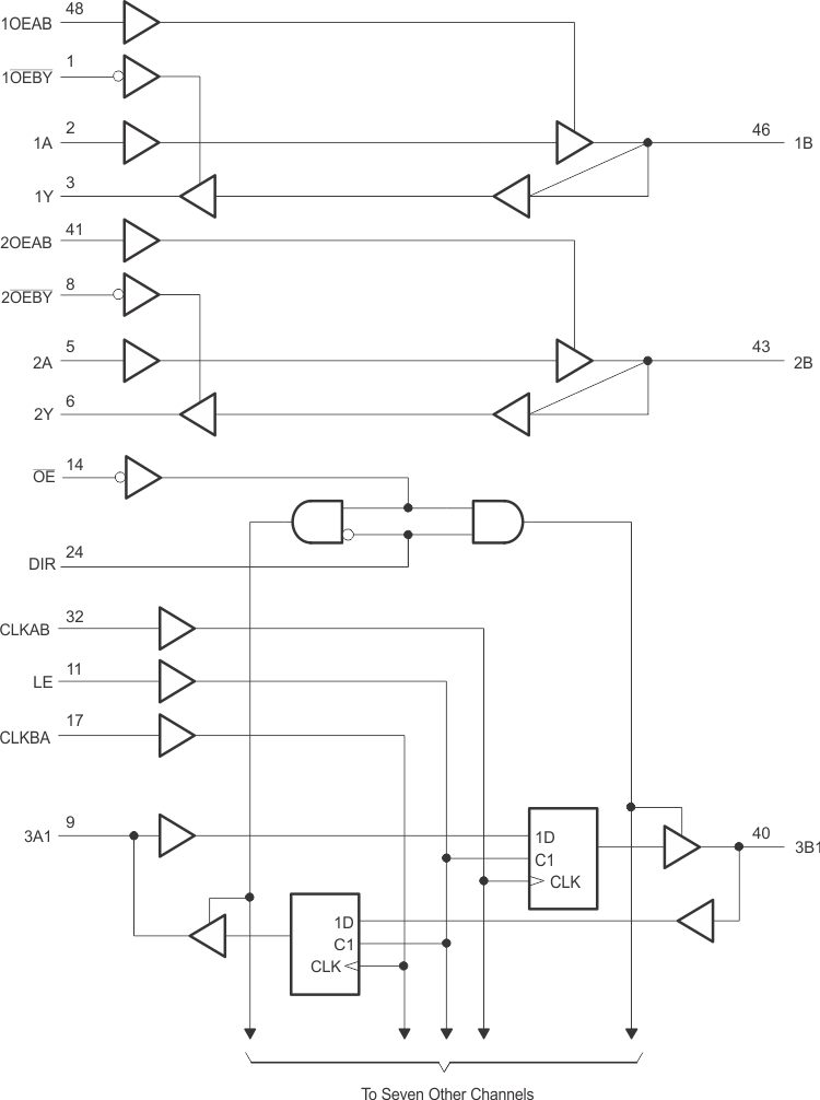
The SN74VMEH22501A-EP 8-bit universal bus transceiver has two integral 1-bit three-wire
bus transceivers and is designed for 3.3-V VCC operation with 5-V tolerant
inputs. The UBT transceiver allows transparent, latched, and flip-flop modes of data transfer, and
the separate LVTTL input and outputs on the bus transceivers provide a feedback path for control
and diagnostics monitoring. This device provides a high-speed interface between cards operating at
LVTTL logic levels and VME64, VME64x, or VME320(2) backplane topologies.The SN74VMEH22501A-EP device is pin-for-pin compatible to the SN74VMEH22501 device
(SCES357), but operates at a wider operating temperature range.High-speed backplane operation is a direct result of the improved OEC circuitry and high
drive that has been designed and tested into the VME64x backplane model. The B-port I/Os are
optimized for driving large capacitive loads and include pseudo-ETL input thresholds (½
VCC ±50 mV) for increased noise immunity. These specifications support the
2eVME protocols in VME64x (ANSI/VITA 1.1) and 2eSST protocols in VITA 1.5. With proper design of a 21-slot VME system, a designer can achieve 320-MB transfer rates
on linear backplanes and, possibly, 1-GB transfer rates on the VME320 backplane.All inputs and outputs are 5-V tolerant and are compatible with TTL and 5-V CMOS
inputs.Active bus-hold circuitry holds unused or undriven 3A-port inputs at a valid logic state.
Bus-hold circuitry is not provided on 1A or 2A inputs, any B-port input, or any control input. Use
of pullup or pulldown resistors with the bus-hold circuitry is not recommended.This device is fully specified for live-insertion applications using
Ioff, power-up 3-state, and BIAS VCC. The
Ioff circuitry prevents damaging current to backflow through the device when
it is powered off/on. The power-up 3-state circuitry places the outputs in the high-impedance state
during power up and power down, which prevents driver conflict. The BIAS VCC
circuitry precharges and preconditions the B-port input/output connections, preventing disturbance
of active data on the backplane during card insertion or removal, and permits true live-insertion
capability.When VCC is between 0 and 1.5 V, the device is in the
high-impedance state during power up or power down. However, to ensure the high-impedance state
above 1.5 V, output-enable (OE and OEBY) inputs
should be tied to VCC through a pullup resistor and output-enable (OEAB)
inputs should be tied to GND through a pulldown resistor; the minimum value of the resistor is
determined by the drive capability of the device connected to this input.
V62/05606-01YE 电路图
V62/05606-01YE 电路图
V62/05606-01YE 相关产品
- 100301QC
- 100304QC
- 100310QC
- 100311QC
- 100313QC
- 100316QC
- 100322QC
- 100329APC
- 100329DC
- 100336DC
- 100336PC
- 100341QC
- 100351DC
- 100351PC
- 100363QC
- 100364QC
- 100370QC
- 100390QC
- 100398QI
- 11AA010T-I/TT
- 11AA160T-I/TT
- 11LC010T-I/TT
- 11LC020T-I/TT
- 11LC040T-E/TT
- 11LC160T-E/TT
- 1ED020I12-F
- 2304NZGI-1LF
- 23A640-I/SN
- 23K256-I/SN
- 23K256-I/ST