 搜索
搜索
 发布采购
发布采购
- RoHS:
• 镉(Cd)/镉化合物 0.01%
• 六价隔(Cr6+)/六价隔化合物 0.10%
• 铅(Pb)/铅化合物 0.10%
• 汞(Hg)/汞化合物 0.10%
• 多溴联苯(PBB)0.10%
• 多溴联苯醚(PBDE)0.10% - 含十溴二苯醚(Deca-BDE) 0.10%
说明:Specialty Function Logic Mil Enh 3.3V ABT Scan Test Devices - 参考价格:¥70.79-¥74.45
更新日期:2024-04-01 00:04:00
产品简介:增强型产品,具有 18 位通用总线收发器的 3.3V Abt 扫描测试设备
查看详情- RoHS:
• 镉(Cd)/镉化合物 0.01%
• 六价隔(Cr6+)/六价隔化合物 0.10%
• 铅(Pb)/铅化合物 0.10%
• 汞(Hg)/汞化合物 0.10%
• 多溴联苯(PBB)0.10%
• 多溴联苯醚(PBDE)0.10% - 含十溴二苯醚(Deca-BDE) 0.10%
说明:Specialty Function Logic Mil Enh 3.3V ABT Scan Test Devices - 参考价格:¥70.79-¥74.45
V62/04730-01XE 中文资料属性参数
- 制造商:Texas Instruments
- 产品种类:特定功能逻辑
- 工作电源电压:3.3 V
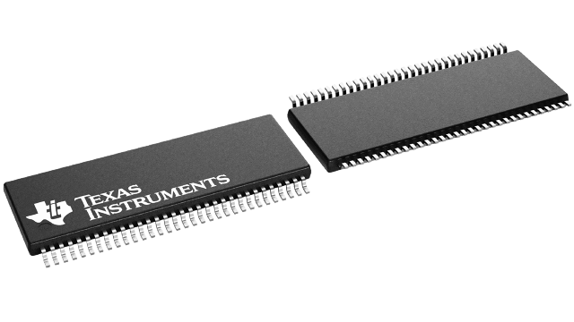
- 封装 / 箱体:TSSOP-64
- 封装:Reel
- 安装风格:SMD/SMT
- 工作温度范围:+ 85 C
- 工厂包装数量:2000
产品特性
- Controlled Baseline One Assembly/Test Site, One Fabrication Site
- One Assembly/Test Site, One Fabrication Site
- Enhanced Diminishing Manufacturing Sources (DMS) Support
- Enhanced Product-Change Notification
- Qualification Pedigree
- Members of the Texas Instruments SCOPE™ Family of Testability Products
- Members of the Texas Instruments Widebus™ Family
- State-of-the-Art 3.3-V ABT Design Supports Mixed-Mode Signal Operation (5-V Input and Output Voltages With 3.3-V VCC)
- Support Unregulated Battery Operation Down to 2.7 V
- UBT™ (Universal Bus Transceiver) Combines D-Type Latches and D-Type Flip-Flops for Operation in Transparent, Latched, or Clocked Mode
- Bus Hold on Data Inputs Eliminates the Need for External Pullup/Pulldown Resistors
- B-Port Outputs of SN74LVTH182512 Device Has Equivalent 25- Series Resistors, So No External Resistors Are Required
- SCOPE™ Instruction Set IEEE Std 1149.1-1990 Required Instructions and Optional CLAMP and HIGHZ Parallel-Signature Analysis at Inputs Pseudo-Random Pattern Generation From Outputs Sample Inputs/Toggle Outputs Binary Count From Outputs Device Identification Even-Parity Opcodes
- IEEE Std 1149.1-1990 Required Instructions and Optional CLAMP and HIGHZ
- Parallel-Signature Analysis at Inputs
- Pseudo-Random Pattern Generation From Outputs
- Sample Inputs/Toggle Outputs
- Binary Count From Outputs
- Device Identification
- Even-Parity Opcodes
- Compatible With the IEEE Std 1149.1-1990 (JTAG) Test Access Port and Boundary-Scan Architecture
产品概述
The SN74LVTH18512 and SN74LVTH182512 scan test devices with 18-bit universal bus transceivers are members of the Texas Instruments SCOPE™ testability integrated-circuit family. This family of devices supports IEEE Std 1149.1-1990 boundary scan to facilitate testing of complex circuit-board assemblies. Scan access to the test circuitry is accomplished via the 4-wire test access port (TAP) interface.Additionally, these devices are designed specifically for low-voltage (3.3-V) VCC operation, but with the capability to provide a TTL interface to a 5-V system environment.In the normal mode, these devices are 18-bit universal bus transceivers that combine D-type latches and D-type flip-flops to allow data flow in transparent, latched, or clocked modes. They can be used either as two 9-bit transceivers or one 18-bit transceiver. The test circuitry can be activated by the TAP to take snapshot samples of the data appearing at the device pins or to perform a self test on the boundary-test cells. Activating the TAP in the normal mode does not affect the functional operation of the SCOPE™ universal bus transceivers.Data flow in each direction is controlled by output-enable (OEAB\ and OEBA\), latch-enable (LEAB and LEBA), and clock (CLKAB and CLKBA) inputs. For A-to-B data flow, the devices operate in the transparent mode when LEAB is high. When LEAB is low, the A data is latched while CLKAB is held at a static low or high logic level. Otherwise, if LEAB is low, A data is stored on a low-to-high transition of CLKAB. When OEAB\ is low, the B outputs are active. When OEAB\ is high, the B outputs are in the high-impedance state. B-to-A data flow is similar to A-to-B data flow but uses the OEBA\, LEBA, and CLKBA inputs.In the test mode, the normal operation of the SCOPE™ universal bus transceivers is inhibited, and the test circuitry is enabled to observe and control the I/O boundary of the device. When enabled, the test circuitry performs boundary-scan test operations according to the protocol described in IEEE Std 1149.1-1990.Four dedicated test pins are used to observe and control the operation of the test circuitry: test data input (TDI), test data output (TDO), test mode select (TMS), and test clock (TCK). Additionally, the test circuitry performs other testing functions such as parallel-signature analysis (PSA) on data inputs and pseudo-random pattern generation (PRPG) from data outputs. All testing and scan operations are synchronized to the TAP interface.Active bus-hold circuitry is provided to hold unused or floating data inputs at a valid logic level.The B-port outputs of SN74LVTH182512, which are designed to source or sink up to 12 mA, include equivalent 25- series resistors to reduce overshoot and undershoot.
V62/04730-01XE 相关产品
- 100301QC
- 100304QC
- 100310QC
- 100311QC
- 100313QC
- 100316QC
- 100322QC
- 100329APC
- 100329DC
- 100336DC
- 100336PC
- 100341QC
- 100351DC
- 100351PC
- 100363QC
- 100364QC
- 100370QC
- 100390QC
- 100398QI
- 11AA010T-I/TT
- 11AA160T-I/TT
- 11LC010T-I/TT
- 11LC020T-I/TT
- 11LC040T-E/TT
- 11LC160T-E/TT
- 1ED020I12-F
- 2304NZGI-1LF
- 23A640-I/SN
- 23K256-I/SN
- 23K256-I/ST