 搜索
搜索
 发布采购
发布采购
- 封装:32-VFQFN 裸露焊盘
- RoHS:无铅 / 符合限制有害物质指令(RoHS)规范要求
- 包装方式:Digi-Reel®
- 参考价格:$5.8255-$7.87
更新日期:2024-04-01 00:04:00
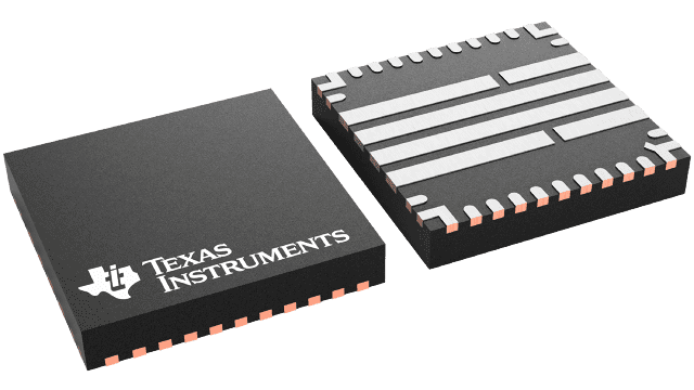
产品简介:数字双通道同步降压功率驱动器
查看详情- 封装:32-VFQFN 裸露焊盘
- RoHS:无铅 / 符合限制有害物质指令(RoHS)规范要求
- 包装方式:Digi-Reel®
- 参考价格:$5.8255-$7.87
UCD7242RSJT 供应商
- 公司
- 型号
- 品牌
- 封装/批号
- 数量
- 地区
- 日期
- 说明
- 询价
-
TI
-
原厂原装
22+ -
3288
-
上海市
-
-
-
一级代理原装
-
TI
-
QFN-32
21+ -
2000
-
上海市
-
-
-
原装现货,品质为先,请来电垂询!
-
TI
-
原厂原封装
新批号 -
887000
-
上海市
-
-
-
原厂发货进口原装微信同步QQ893727827
-
TI
-
TSSOP
23+ -
46000
-
合肥
-
-
-
科大讯飞战略投资企业,提供一站式配套服务
UCD7242RSJT 中文资料属性参数
- 标准包装:1
- 类别:集成电路 (IC)
- 家庭:PMIC - 稳压器 - DC DC 开关稳压器
- 系列:-
- 类型:降压(降压)
- 输出类型:-
- 输出数:2
- 输出电压:-
- 输入电压:4.75 V ~ 18 V
- PWM 型:-
- 频率 - 开关:300kHz ~ 2MHz
- 电流 - 输出:10A
- 同步整流器:是
- 工作温度:-40°C ~ 125°C
- 安装类型:表面贴装
- 封装/外壳:32-VFQFN 裸露焊盘
- 包装:®
- 供应商设备封装:32-QFN(6x6)
- 其它名称:296-27191-6
产品特性
- Fully Integrated Power Switches With Drivers for Dual Synchronous Buck Converters
- Full Compatibility With TI Fusion Digital Power Supply Controllers, Such as the UCD92xx Family
- Wide Input Voltage Range: 4.75 V to 18 V Operational Down to 2.2 V Input With an External Bias Supply
- Up to 10A Output Current per Channel
- Operational to 2 MHz Switching Frequency
- High Side Current Limit With Current Limit Flag
- Onboard Regulated 6 V Driver Supply From VIN
- Thermal Protection
- Temperature Sense Output – Voltage Proportional to Chip Temperature
- UVLO and OVLO Circuits Ensure Proper Drive Voltage
- Rated From –40°C to 125°C Junction Temperature
- RoHS Compliant
- Accurate On-Die Current Sensing (±5%)
- APPLICATIONS Digitally-Controlled Synchronous-Buck Power Stages High Current Dual-Phase VRM/EVRD Regulators for Desktop, Server, Telecom and Notebook Processors
- Digitally-Controlled Synchronous-Buck Power Stages
- High Current Dual-Phase VRM/EVRD Regulators for Desktop, Server, Telecom and Notebook Processors
产品概述
The UCD7242 is a complete power system ready to drive two independent buck power supplies. High side MOSFETs, low side MOSFETs, drivers, current sensing circuitry and necessary protection functions are all integrated into one monolithic solution to facilitate minimum size and maximum efficiency. Driver circuits provide high charge and discharge current for the high-side NMOS switch and the low-side NMOS synchronous rectifier in a synchronous buck circuit. The MOSFET gates are driven to +6.25 V by an internally regulated VGG supply. The internal VGG regulator can be disabled to permit the user to supply an independent gate drive voltage. This flexibility allows a wide power conversion input voltage range of 2.2V to 18V. Internal under voltage lockout (UVLO) logic ensures VGG is good before allowing chip operation.The synchronous rectifier enable (SRE) pin controls whether or not the low-side MOSFET is
turned on when the PWM signal is low. When SRE is high the part operates in continuous conduction
mode for all loads. In this mode the drive logic block uses the PWM signal to control both the
high-side and low-side gate drive signals. Dead time is also optimized to prevent cross conduction.
When SRE is low, the part operates in discontinuous conduction mode at light loads. In this mode
the low-side MOSFET is always held off. On-board comparators monitor the current through the high side switch to safeguard the
power stage from sudden high current loads. Blanking delay is set for the high side comparator to
avoid false reports coincident with switching edge noise. In the event of an over-current fault,
the high-side FET is turned off and the Fault Flag (FLT) is asserted to alert the controller.MOSFET current is measured and monitored by a precision integrated current sense element.
This method provides an accuracy of ±5% over most of the load range. The amplified signal is
available for use by the controller on the IMON pin.An on-chip temperature sense converts the die temperature to a voltage at the
TMON pin for the controller’s use. If the die temperature exceeds 170°C, the
temperature sensor initiates a thermal shutdown that halts output switching and sets the FLT flag.
Normal operation resumes when the die temperature falls below the thermal hysteresis band.
UCD7242RSJT 数据手册
| 数据手册 | 说明 | 数量 | 操作 |
|---|---|---|---|
 UCD7242RSJT UCD7242RSJT
|
Buck Switching Regulator IC Positive 2 Output 10A 32-PowerVFQFN |
36页,2.1M | 查看 |
UCD7242RSJT 电路图
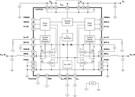
UCD7242RSJT 电路图
UCD7242RSJT 相关产品
- A5970D013TR
- A5975DTR
- A7986ATR
- ADM660ARUZ
- ADM660ARUZ-REEL
- ADM660ARZ
- ADM660ARZ-REEL
- ADM8660ANZ
- ADM8660ARZ-REEL
- ADM8828ART-REEL
- ADM8828ARTZ-REEL
- ADM8829ARTZ-REEL
- ADP1111ARZ
- ADP1111ARZ-3.3
- ADP2102YCPZ-1.2-R7
- ADP2102YCPZ-2-R7
- ADP2102YCPZ-3-R7
- ADP2102YCPZ-4-R7
- ADP2105ACPZ-1.2-R7
- ADP2105ACPZ-1.8-R7
- ADP2105ACPZ-3.3-R7
- ADP2105ACPZ-R7
- ADP2106ACPZ-R7
- ADP2107ACPZ-3.3-R7
- ADP2107ACPZ-R7
- ADP2108AUJZ-1.0-R7
- ADP2108AUJZ-1.8-R7
- ADP2108AUJZ-3.3-R7
- ADP2114ACPZ-R7
- ADP2119ACPZ-1.0-R7