 搜索
搜索
 发布采购
发布采购
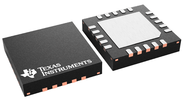
- 封装:20-WFQFN 裸露焊盘
- RoHS:无铅 / 符合限制有害物质指令(RoHS)规范要求
- 包装方式:带卷 (TR)
- 参考价格:$0.81
更新日期:2024-04-01 00:04:00
产品简介:具有电流感应和故障保护功能的数字控制兼容同步降压闸极驱动器
查看详情- 封装:20-WFQFN 裸露焊盘
- RoHS:无铅 / 符合限制有害物质指令(RoHS)规范要求
- 包装方式:带卷 (TR)
- 参考价格:$0.81
UCD7231RTJR 供应商
- 公司
- 型号
- 品牌
- 封装/批号
- 数量
- 地区
- 日期
- 说明
- 询价
-
TI
-
原厂原装
22+ -
3288
-
上海市
-
-
-
一级代理原装
-
TI(德州仪器)
-
QFN-20(4x4)
2022+ -
12000
-
上海市
-
-
-
原装可开发票
-
TI
-
原厂原封装
新批号 -
887000
-
上海市
-
-
-
原厂发货进口原装微信同步QQ893727827
-
TI
-
QFN20
23+ -
5800
-
上海市
-
-
-
进口原装现货,杜绝假货。
UCD7231RTJR 中文资料属性参数
- 标准包装:3,000
- 类别:集成电路 (IC)
- 家庭:PMIC - 稳压器 - DC DC 切换控制器
- 系列:-
- PWM 型:控制器
- 输出数:1
- 频率 - 最大:2MHz
- 占空比:-
- 电源电压:4.7 V ~ 15 V
- 降压:是
- 升压:无
- 回扫:无
- 反相:无
- 倍增器:无
- 除法器:无
- Cuk:无
- 隔离:无
- 工作温度:-40°C ~ 125°C
- 封装/外壳:20-WFQFN 裸露焊盘
- 包装:带卷 (TR)
产品特性
- Dual High Current Drivers.
- Full Compatibility with TI Fusion Digital Power Supply Controllers, such as UCD91xx and UCD92xx Families
- Operational to 2 MHz Switching Frequency
- High-Side FET and Output Current Limit Protection with Independently Adjustable Thresholds
- Fast High-Side Over-Current Sense Circuit with Fault Flag Output – Prevents Catastrophic Current Levels on a Cycle by Cycle Basis
- Differential High-Gain Current Sense Amplifier
- Voltage Proportional to Load Current Monitor Output
- Wide Input Voltage Range: 4.7 V to 15 VOperation to 2.2 V Input Supported with an External 4.5-6.5 V Bias Supply
- Onboard Regulated Supplies for Gate Drive and Internal Circuits
- Integrated Thermal Shutdown
- Selectable Operation Modes:PWM plus Synchronous Rectifier Enable (SRE) with Automatic Dead-Time ControlDirect High-Gate and Low-Gate Inputs for Direct FET Control
- PWM plus Synchronous Rectifier Enable (SRE) with Automatic Dead-Time Control
- Direct High-Gate and Low-Gate Inputs for Direct FET Control
- 3-State PWM Input for Power Stage Shutdown
- UVLO Housekeeping Circuit
- Rated from –40°C to +125°C Junction Temperature
- Pb (Lead) Free Packaging
- APPLICATIONS Digitally-Controlled Synchronous-Buck Power Stages for Single- and Multi-Phase Applications Digitally-Controlled Power Modules
- Digitally-Controlled Synchronous-Buck Power Stages for Single- and Multi-Phase Applications
- Digitally-Controlled Power Modules
产品概述
The UCD7231 high current driver is specifically designed for digitally-controlled, point-of-load, synchronous buck switching power supplies. Two driver circuits provide high charge and discharge current for the high-side NMOS switch and the low-side NMOS synchronous rectifier in a synchronous buck circuit. The MOSFET gates are driven to +6 V by an internally regulated VGG supply. The internal VGG regulator can be disabled to permit the user to supply their own gate drive voltage. This flexibility allows a wide power conversion input voltage range of 2.2 to 15 V. Internal under voltage lockout (UVLO) logic insures VGG is good before allowing chip operation.A drive logic block allows operation in one of two modes selected by the SRE Mode pin. In Synchronous Mode, the logic block uses the PWM signal to control both the high-side and low-side gate drive signals. Dead time is automatically adjusted to prevent cross conduction. The Synchronous Rectifier Enable (SRE) pin controls whether or not the low-side FET is turned on when the PWM signal is low. In Independent Mode, the PWM and SRE pins control the high-side and low-side gates directly. No anti-cross-conduction logic is used in this mode. On-board comparators monitor the voltage across the high side switch and the voltage across an external current sense element to safeguard the power stage from sudden high current loads. Blanking delay is set for the high side comparator by a single resistor in order to avoid false reports coincident with switching edge noise. In the event of a high-side fault or an over-current fault, the high-side FET turned off and the Fault Flag (FLT) is asserted to alert the digital controller. The fault thresholds are independently set by the HS Sense and ILIM pins.Output current is measured and monitored by a precision, high gain, switched capacitor differential amplifier that processes the voltage present across an external current sense element. The amplified signal is available for use by the digital controller on the IMON pin. The current sense amplifier has output offset of 0.5 V so that both positive (sourcing) and negative (sinking) current can be sensed.An on-chip temperature sense monitors the die temperature. If it exceeds approximately 165°C, the temperature sensor will initiate a thermal shutdown that halts output switching and sets the FLT flag. The temperature fault automatically clears when the die temperatures falls by approximately 20°.
UCD7231RTJR 相关产品
- ADP1621ARMZ-R7
- ADP1822ARQZ-R7
- ADP1829ACPZ-R7
- ADP1850ACPZ-R7
- ADP1864AUJZ-R7
- ADP1870ACPZ-0.3-R7
- ADP1870ACPZ-1.0-R7
- ADP1870ARMZ-0.3-R7
- ADP1870ARMZ-0.6-R7
- ADP1870ARMZ-1.0-R7
- ADP1871ACPZ-0.3-R7
- ADP1871ACPZ-0.6-R7
- ADP1871ACPZ-1.0-R7
- ADP1871ARMZ-0.3-R7
- ADP1871ARMZ-0.6-R7
- ADP1871ARMZ-1.0-R7
- ADP1874ARQZ-0.3-R7
- ADP1875ARQZ-0.3-R7
- ADP1876ACPZ-R7
- ADP1878ACPZ-0.3-R7
- ADP1882ARMZ-0.3-R7
- ADP1882ARMZ-0.6-R7
- ADP1882ARMZ-1.0-R7
- ADP1883ARMZ-0.3-R7
- ADP1883ARMZ-0.6-R7
- ADP1883ARMZ-1.0-R7
- ADP2323ACPZ-R7
- ADP2325ACPZ-R7
- AN8016NSH-E1
- AN8018SA-E1