 搜索
搜索
 发布采购
发布采购
- 封装:SOT-23-6 细型,TSOT-23-6
- RoHS:无铅 / 符合限制有害物质指令(RoHS)规范要求
- 包装方式:Digi-Reel®
- 参考价格:$1.4155-$3.03
更新日期:2024-04-01 00:04:00
产品简介:采用 ThinSOT-23 封装且具有强制 PWM 模式的可调节 600mA 开关、1200kHz 升压转换器
查看详情- 封装:SOT-23-6 细型,TSOT-23-6
- RoHS:无铅 / 符合限制有害物质指令(RoHS)规范要求
- 包装方式:Digi-Reel®
- 参考价格:$1.4155-$3.03
TPS61071TDDCRQ1 供应商
- 公司
- 型号
- 品牌
- 封装/批号
- 数量
- 地区
- 日期
- 说明
- 询价
-
TI
-
原厂原装
22+ -
3288
-
上海市
-
-
-
一级代理原装
-
TI/德州仪器
-
SC70-6
2024 -
91752
-
上海市
-
-
-
上海原装现货库存,欢迎咨询合作
-
-
23+ -
46000
-
合肥
-
-
-
科大讯飞战略投资企业,提供一站式配套服务
TPS61071TDDCRQ1 中文资料属性参数
- 标准包装:1
- 类别:集成电路 (IC)
- 家庭:PMIC - 稳压器 - DC DC 开关稳压器
- 系列:-
- 类型:升压(升压)
- 输出类型:可调式
- 输出数:1
- 输出电压:1.8 V ~ 5.5 V
- 输入电压:0.9 V ~ 5.5 V
- PWM 型:-
- 频率 - 开关:1.2MHz
- 电流 - 输出:600mA
- 同步整流器:是
- 工作温度:-40°C ~ 105°C
- 安装类型:表面贴装
- 封装/外壳:SOT-23-6 细型,TSOT-23-6
- 包装:®
- 供应商设备封装:6-SOT
- 其它名称:296-27690-6
产品特性
- Qualified for Automotive Applications
- AEC-Q100 Qualified With the Following Results: Device Temperature Grade 2: –40°C to 105°C Ambient Operating Temperature Range Device HBM Classification Level 1C Device CDM Classification Level C6
- Device Temperature Grade 2: –40°C to 105°C Ambient Operating Temperature Range
- Device HBM Classification Level 1C
- Device CDM Classification Level C6
- 90% Efficient Synchronous Boost Converter 75-mA Output Current at 3.3 V From 0.9-V Input 150-mA Output Current at 3.3 V From 1.8-V Input
- 75-mA Output Current at 3.3 V From 0.9-V Input
- 150-mA Output Current at 3.3 V From 1.8-V Input
- Device Quiescent Current: 19 µA (Typical)
- Input Voltage Range: 0.9 V to 5.5 V
- Adjustable Output Voltage Up to 5.5 V
- Power-Save Mode Version Available for Improved Efficiency at Low Output Power
- Load Disconnect During Shutdown
- Overtemperature Protection
- Small 6-Pin Thin SOT Package
产品概述
The TPS61071-Q1 device provides a power supply solution for products powered by
lower-voltage DC rails or a one-cell, two-cell, or three-cell alkaline, NiCd or NiMH, or one-cell
Li-ion or Li-polymer battery. Output currents can go as high as 75 mA, while using a single-cell
alkaline, and discharge down to 0.9 V. The device can also generate 5 V at 200 mA from a 3.3-V rail
or a Li-ion battery. The boost converter is based on a fixed frequency, pulse-width-modulation
(PWM) controller using a synchronous rectifier to obtain maximum efficiency. The maximum peak
current in the boost switch is limited typically to a value of 600 mA.The TPS61071-Q1 output voltage is programmed by an external resistor divider. To minimize
battery drain, disable the converter. During shutdown, the load disconnects from the battery. The
device package is a 6-pin thin SOT package (DDC).
TPS61071TDDCRQ1 电路图
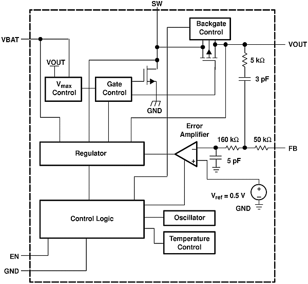
TPS61071TDDCRQ1 电路图
TPS61071TDDCRQ1 相关产品
- A5970D013TR
- A5975DTR
- A7986ATR
- ADM660ARUZ
- ADM660ARUZ-REEL
- ADM660ARZ
- ADM660ARZ-REEL
- ADM8660ANZ
- ADM8660ARZ-REEL
- ADM8828ART-REEL
- ADM8828ARTZ-REEL
- ADM8829ARTZ-REEL
- ADP1111ARZ
- ADP1111ARZ-3.3
- ADP2102YCPZ-1.2-R7
- ADP2102YCPZ-2-R7
- ADP2102YCPZ-3-R7
- ADP2102YCPZ-4-R7
- ADP2105ACPZ-1.2-R7
- ADP2105ACPZ-1.8-R7
- ADP2105ACPZ-3.3-R7
- ADP2105ACPZ-R7
- ADP2106ACPZ-R7
- ADP2107ACPZ-3.3-R7
- ADP2107ACPZ-R7
- ADP2108AUJZ-1.0-R7
- ADP2108AUJZ-1.8-R7
- ADP2108AUJZ-3.3-R7
- ADP2114ACPZ-R7
- ADP2119ACPZ-1.0-R7