 搜索
搜索
 发布采购
发布采购
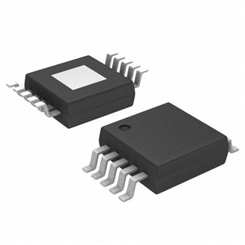
- 封装:10-TFSOP,10-MSOP(0.118",3.00mm 宽)裸露焊盘
- RoHS:无铅 / 符合限制有害物质指令(RoHS)规范要求
- 包装方式:Digi-Reel®
- 参考价格:$3.096-$6.19
更新日期:2025-03-27 14:03:14
产品简介:具有 Eco-Mode™ 的汽车类 3.5V 至 42V、2.5A 降压转换器
查看详情- 封装:10-TFSOP,10-MSOP(0.118",3.00mm 宽)裸露焊盘
- RoHS:无铅 / 符合限制有害物质指令(RoHS)规范要求
- 包装方式:Digi-Reel®
- 参考价格:$3.096-$6.19
TPS54240QDGQRQ1 供应商
- 公司
- 型号
- 品牌
- 封装/批号
- 数量
- 地区
- 日期
- 说明
- 询价
-
TPS54240QDGQRQ1
原装现货 -
TI
-
MSOP10
22+ -
2662
-
深圳
-
03-27
-
????
-
TI
-
原厂原装
22+ -
3288
-
上海市
-
-
-
一级代理原装
-
TI(德州仪器)
-
HVSSOP-10
2022+ -
145
-
上海市
-
-
-
原装可开发票
-
TI
-
MSOP
21+ -
20000
-
上海市
-
-
-
原装现货,品质为先!请来电垂询!
-
TSSOP
23+ -
46000
-
合肥
-
-
-
科大讯飞战略投资企业,提供一站式配套服务
TPS54240QDGQRQ1 中文资料属性参数
- 标准包装:1
- 类别:集成电路 (IC)
- 家庭:PMIC - 稳压器 - DC DC 开关稳压器
- 系列:SWIFT™, Eco-Mode™
- 类型:降压(降压)
- 输出类型:可调式
- 输出数:1
- 输出电压:0.8 V ~ 39 V
- 输入电压:3.5 V ~ 42 V
- PWM 型:电流模式
- 频率 - 开关:100kHz ~ 2.5MHz
- 电流 - 输出:2.5A
- 同步整流器:无
- 工作温度:-40°C ~ 125°C
- 安装类型:表面贴装
- 封装/外壳:10-TFSOP,10-MSOP(0.118",3.00mm 宽)裸露焊盘
- 包装:®
- 供应商设备封装:10-MSOP-PowerPad
- 其它名称:296-28182-6
产品特性
- Qualified for Automotive Applications
- AEC Q100 Qualified With the Following Results: Device Temperature Grade 1: –40°C to 125°C Ambient Operating Temperature Range Device HBM ESD Classification Level H2 Device CDM ESD Classification Level C6
- Device Temperature Grade 1: –40°C to 125°C Ambient Operating Temperature Range
- Device HBM ESD Classification Level H2
- Device CDM ESD Classification Level C6
- 3.5-V to 42-V Input Voltage Range
- 200-mΩ High-Side MOSFET
- High Efficiency at Light Loads With a Pulse-Skipping Eco-mode Control Scheme
- 138-µA Operating Quiescent Current
- 1.3-µA Shutdown Current
- 100-kHz to 2.5-MHz Switching Frequency
- Synchronizes to External Clock
- Adjustable Slow Start/Sequencing
- UV and OV Power-Good Output
- Adjustable UVLO Voltage and Hysteresis
- 0.8-V Internal Voltage Reference
- MSOP10 PowerPAD Package
- Supported by SwitcherPro Software Tool (http://focus.ti.com/docs/toolsw/folders/print/switcherpro.html)
- For SWIFT Documentation, See the TI Web site at http://www.ti.com/swift
产品概述
The TPS54240-Q1 device is a 42-V, 2.5-A, step-down regulator with an integrated high-side
MOSFET. Current-mode control provides simple external compensation and flexible component
selection. A low-ripple pulse-skip mode reduces the no-load, regulated-output supply current to 138
µA. Using the enable pin, shutdown supply current is reduced to 1.3 µA when the enable pin is
low.Undervoltage lockout is internally set at 2.5 V, but can be increased using the enable
pin. The output voltage start-up ramp is controlled by the slow-start pin that can also be
configured for sequencing/tracking. An open-drain power-good signal indicates the output is within
94% to 107% of its nominal voltage.A wide switching-frequency range allows efficiency and external component size to be
optimized. Frequency foldback and thermal shutdown protects the part during an overload
condition.The TPS54240-Q1 is available in a 10-pin thermally enhanced MSOP PowerPAD package.
TPS54240QDGQRQ1 电路图
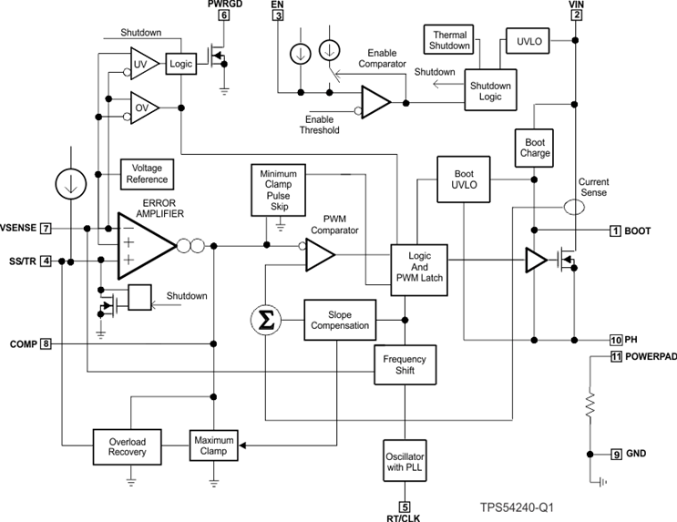
TPS54240QDGQRQ1 电路图
TPS54240QDGQRQ1 相关产品
- A5970D013TR
- A5975DTR
- A7986ATR
- ADM660ARUZ
- ADM660ARUZ-REEL
- ADM660ARZ
- ADM660ARZ-REEL
- ADM8660ANZ
- ADM8660ARZ-REEL
- ADM8828ART-REEL
- ADM8828ARTZ-REEL
- ADM8829ARTZ-REEL
- ADP1111ARZ
- ADP1111ARZ-3.3
- ADP2102YCPZ-1.2-R7
- ADP2102YCPZ-2-R7
- ADP2102YCPZ-3-R7
- ADP2102YCPZ-4-R7
- ADP2105ACPZ-1.2-R7
- ADP2105ACPZ-1.8-R7
- ADP2105ACPZ-3.3-R7
- ADP2105ACPZ-R7
- ADP2106ACPZ-R7
- ADP2107ACPZ-3.3-R7
- ADP2107ACPZ-R7
- ADP2108AUJZ-1.0-R7
- ADP2108AUJZ-1.8-R7
- ADP2108AUJZ-3.3-R7
- ADP2114ACPZ-R7
- ADP2119ACPZ-1.0-R7