 搜索
搜索
 发布采购
发布采购
- 封装:6-XFBGA,DSBGA
- RoHS:无铅 / 符合限制有害物质指令(RoHS)规范要求
- 包装方式:Digi-Reel®
- 参考价格:$0.6955-$1
更新日期:2024-04-01 00:04:00

产品简介:具有输出放电功能的 3.6V、0.5A、55mΩ、80nA 泄漏负载开关
查看详情- 封装:6-XFBGA,DSBGA
- RoHS:无铅 / 符合限制有害物质指令(RoHS)规范要求
- 包装方式:Digi-Reel®
- 参考价格:$0.6955-$1
TPS22932BYFPT 供应商
- 公司
- 型号
- 品牌
- 封装/批号
- 数量
- 地区
- 日期
- 说明
- 询价
-
TI
-
原厂原装
22+ -
3288
-
上海市
-
-
-
一级代理原装
-
TI(德州仪器)
-
DSBGA-6
2022+ -
12000
-
上海市
-
-
-
原装可开发票
-
TI
-
多路器开关IC
21+ -
10000
-
上海市
-
-
-
原装现货,品质为先!请来电垂询!
-
TI
-
原厂原装
2318+ -
9200
-
合肥
-
-
-
科大讯飞战略投资企业
TPS22932BYFPT 中文资料属性参数
- 标准包装:1
- 类别:集成电路 (IC)
- 家庭:PMIC - 电源分配开关
- 系列:-
- 类型:通用
- 输出数:1
- Rds(开):70 毫欧
- 内部开关:是
- 电流限制:500mA
- 输入电压:1.1 V ~ 3.6 V
- 工作温度:-40°C ~ 85°C
- 安装类型:表面贴装
- 封装/外壳:6-XFBGA,DSBGA
- 供应商设备封装:6-DSBGA
- 包装:®
- 其它名称:296-25448-6
产品特性
- Input Voltage: 1.1 V to 3.6 V
- Ultralow ON-Resistance rON = 55 mΩ at VIN = 3.6 V rON = 65 mΩ at VIN = 2.5 V rON = 75 mΩ at VIN = 1.8 V rON = 115 mΩ at VIN = 1.2 V
- rON = 55 mΩ at VIN = 3.6 V
- rON = 65 mΩ at VIN = 2.5 V
- rON = 75 mΩ at VIN = 1.8 V
- rON = 115 mΩ at VIN = 1.2 V
- 500-mA Maximum Continuous Switch Current
- Quiescent Current < 1 µA
- Shutdown Current < 1 µA
- Low Control Threshold Allows Use of 1.2-V, 1.8-V, 2.5-V, and 3.3-V Logic
- Configurable Enable Logic
- Controlled Slew Rate to Avoid Inrush Currents: 165 µs at 1.8 V
- Six-Terminal Wafer Chip Scale Package (DSBGA)
- ESD Performance Tested Per JESD 22 2000-V Human-Body Model (A114-B, Class II) 1000-V Charged-Device Model (C101)
- 2000-V Human-Body Model (A114-B, Class II)
- 1000-V Charged-Device Model (C101)
- APPLICATIONS PDAs Cell Phones GPS Devices MP3 Players Digital Cameras Peripheral Ports Portable Instrumentation
- PDAs
- Cell Phones
- GPS Devices
- MP3 Players
- Digital Cameras
- Peripheral Ports
- Portable Instrumentation
产品概述
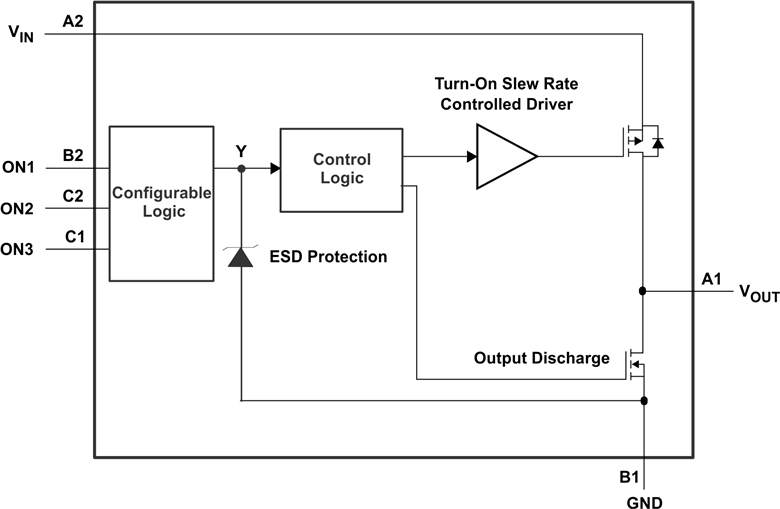
The TPS22932B device is a low rON load switch with controlled
turnon. The device contains a P-channel MOSFET that can operate over an input voltage range of 1.1
V to 3.6 V.The switch is controlled by eight patterns of 3-bit input. The user can choose the logic
functions MUX, AND, OR, NAND, NOR, inverter, and noninverter. All inputs can be connected to
VIN or GND. The control pins can be connected to low-voltage GPIOs allowing
the switch to be controlled by either 1.2-V, 1.8-V, 2.5-V, or 3.3-V logic signals while keeping
extremely low quiescent current.A 120-Ω on-chip load resistor is available for output quick discharge when the switch is
turned off. The rise time (slew rate) of the device is internally controlled to avoid inrush
current: the rise time of TPS22932B is 165 µs.TPS22932B is available in a space-saving 6-pin DSBGA (YFP with 0.4-mm pitch). The device
is characterized for operation over the free-air temperature range of –40°C to 85°C.
TPS22932BYFPT 电路图
TPS22932BYFPT 电路图
TPS22932BYFPT 相关产品
- AOZ1310CI-1
- AOZ1321DI-03L
- AP2101MPG-13
- AP2111SG-13
- AP2156SG-13
- AP2162AMPG-13
- AP2162SG-13
- AP2171MPG-13
- AP2172AMPG-13
- AP2176SG-13
- AP2181WG-7
- AP2280-1FMG-7
- AP2280-2FMG-7
- AP2280-2WG-7
- AP2331SA-7
- AP2401MP-13
- AP2401S-13
- AP2411MP-13
- AP2411S-13
- BD6522F-E2
- FDY6342L
- FPF1009R
- FPF1048BUCX
- FPF1204UCX
- FPF1207UCX
- FPF1208UCX
- FPF1320UCX
- FPF1321UCX
- FPF2193
- FPF2195