 搜索
搜索
 发布采购
发布采购
- 封装:8-TSSOP(0.173",4.40mm 宽)
- RoHS:无铅 / 符合限制有害物质指令(RoHS)规范要求
- 包装方式:Digi-Reel®
- 参考价格:$1.341-$2.87
更新日期:2024-04-01 00:04:00
产品简介:具有手动和自动切换及状态输出功能的 2.8V 至 5.5V、84mΩ、1.25A 汽车类电源多路复用器
查看详情- 封装:8-TSSOP(0.173",4.40mm 宽)
- RoHS:无铅 / 符合限制有害物质指令(RoHS)规范要求
- 包装方式:Digi-Reel®
- 参考价格:$1.341-$2.87
TPS2115AIPWRQ1 供应商
- 公司
- 型号
- 品牌
- 封装/批号
- 数量
- 地区
- 日期
- 说明
- 询价
-
TI
-
TSSOP8
21+ -
2000
-
上海市
-
-
-
原厂原装上海仓现货
-
TI(德州仪器)
-
TSSOP-8
2022+ -
12000
-
上海市
-
-
-
原装可开发票
TPS2115AIPWRQ1 中文资料属性参数
- 标准包装:1
- 类别:集成电路 (IC)
- 家庭:PMIC - O 圈控制器
- 系列:-
- 应用:手持/移动设备
- FET 型:N 沟道
- 输出数:1
- 内部开关:是
- 延迟时间 - 开启:1ms
- 延迟时间 - 关闭:5ms
- 电源电压:2.8 V ~ 5.5 V
- 电流 - 电源:55µA
- 工作温度:-40°C ~ 85°C
- 安装类型:表面贴装
- 封装/外壳:8-TSSOP(0.173",4.40mm 宽)
- 供应商设备封装:8-TSSOP
- 包装:®
- 配用:296-18937-ND - EVAL MODULE FOR TPS2115A-061296-20590-ND - EVAL MOD FOR TPS2115296-20588-ND - EVAL MOD FOR TPS2111296-20589-ND - EVAL MOD FOR TPS2113
- 其它名称:296-24155-6
产品特性
- Qualified for Automotive Applications
- AEC-Q100 Qualified With the Following Results: Device Temperature Grade 3: –40°C to 85°C Ambient Operating Temperature Range Device HBM ESD Classification Level 2 Device CDM ESD Classification Level C4A
- Device Temperature Grade 3: –40°C to 85°C Ambient Operating Temperature Range
- Device HBM ESD Classification Level 2
- Device CDM ESD Classification Level C4A
- Two-Input One-Output Power Multiplexer With Low rDS(on) Switch...84 mΩ (Typical)
- Reverse and Cross-Conduction Blocking
- Wide Operating Voltage Range...2.8 V to 5.5 V
- Low Standby Current...0.5 µA (Typical)
- Low Operating Current...55 µA (Typical)
- Adjustable Current Limit
- Controlled Output-Voltage Transition Times Limit Inrush Current and Minimize Output Voltage Hold- Up Capacitance
- CMOS- and TTL-Compatible Control Inputs
- Manual and Auto-Switching Operating Modes
- Thermal Shutdown
- Available in TSSOP-8 (PW) Package
产品概述
The
TPS2115A-Q1 power multiplexer enables seamless
transition between two power supplies, such as a two supply rails or a battery and AC to DC wall
adapter. Each supply operates at 2.8 V to 5.5 V and the output can deliver up to 1 A. The
TPS2115A-Q1 device includes extensive protection circuitry including user-programmable current
limiting, thermal protection, inrush current control, seamless supply transition, cross-conduction
blocking, and reverse-conduction blocking. These features greatly simplify designing power
multiplexer applications.
TPS2115AIPWRQ1 电路图
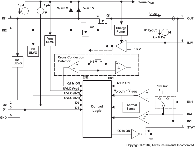
TPS2115AIPWRQ1 电路图
TPS2115AIPWRQ1 相关产品
- CAT6500HVA-T2
- IR5001STRPBF
- ISL6144IVZA-T7A
- ISL6146AFRZ-T7A
- ISL6146BFRZ
- LTC4352HDD#PBF
- LTC4352HMS#PBF
- LTC4355CDE#PBF
- LTC4355IDE#PBF
- LTC4357CMS8#PBF
- LTC4357MPMS8
- LTC4357MPMS8#PBF
- LTC4370CMS#PBF
- LTC4412ES6#TR
- LTC4412ES6#TRMPBF
- LTC4415EDHC#PBF
- LTC4415EMSE#PBF
- LTC4415IDHC#PBF
- LTC4415IMSE#PBF
- MAX5944ESE+
- TPS2100DBVR
- TPS2100DBVT
- TPS2101D
- TPS2101DBVR
- TPS2101DBVT
- TPS2102DBVR
- TPS2103DBVR
- TPS2103DBVT
- TPS2104DBVR
- TPS2104DBVT