 搜索
搜索
 发布采购
发布采购
更新日期:2024-04-01 00:04:00

产品简介:16/32 位 RISC 闪存 MCU,Cortex R4F,通过 Q100 车规认证,EMAC
查看详情TMS5701227CPGEQQ1 供应商
- 公司
- 型号
- 品牌
- 封装/批号
- 数量
- 地区
- 日期
- 说明
- 询价
-
TI
-
原厂原装
22+ -
3288
-
上海市
-
-
-
一级代理原装
TMS5701227CPGEQQ1 中文资料属性参数
- 现有数量:0现货查看交期
- 价格:1 : ¥200.81000托盘
- 系列:Automotive, AEC-Q100, Hercules? TMS570 ARM? Cortex?-R
- 包装:托盘
- 产品状态:在售
- 核心处理器:ARM? Cortex?-R4F
- 内核规格:32 位双核
- 速度:160MHz
- 连接能力:CANbus,EBI/EMI,以太网,FlexRay,I2C,LINbus,MibSPI,SPI,CI,ART/USART
- 外设:DMA,POR,PWM,WDT
- I/O 数:58
- 程序存储容量:1.25MB(1.25M x 8)
- 程序存储器类型:闪存
- EEPROM 容量:64K x 8
- RAM 大小:192K x 8
- 电压 - 供电 (Vcc/Vdd):1.14V ~ 3.6V
- 数据转换器:A/D 24x12b
- 振荡器类型:外部
- 工作温度:-40°C ~ 125°C(TA)
- 安装类型:表面贴装型
- 封装/外壳:144-LQFP
- 供应商器件封装:144-LQFP(20x20)
产品特性
- High-Performance Automotive-Grade Microcontroller for Safety-Critical ApplicationsDual CPUs Running in Lockstep ECC on Flash and RAM Interfaces Built-In Self-Test (BIST) for CPU and On-chip RAMs Error Signaling Module With Error Pin Voltage and Clock Monitoring
- Dual CPUs Running in Lockstep
- ECC on Flash and RAM Interfaces
- Built-In Self-Test (BIST) for CPU and On-chip RAMs
- Error Signaling Module With Error Pin
- Voltage and Clock Monitoring
- ARM Cortex-R4F 32-Bit RISC CPU 1.66 DMIPS/MHz With 8-Stage Pipeline FPU With Single- and Double-Precision 12-Region Memory Protection Unit (MPU) Open Architecture With Third-Party Support
- 1.66 DMIPS/MHz With 8-Stage Pipeline
- FPU With Single- and Double-Precision
- 12-Region Memory Protection Unit (MPU)
- Open Architecture With Third-Party Support
- Operating ConditionsUp to 180-MHz System Clock Core Supply Voltage (VCC): 1.14 to 1.32 V I/O Supply Voltage (VCCIO): 3.0 to 3.6 V
- Up to 180-MHz System Clock
- Core Supply Voltage (VCC): 1.14 to 1.32 V
- I/O Supply Voltage (VCCIO): 3.0 to 3.6 V
- Integrated Memory1.25MB of Program Flash With ECC 192KB of RAM With ECC 64KB of Flash for Emulated EEPROM With ECC
- 1.25MB of Program Flash With ECC
- 192KB of RAM With ECC
- 64KB of Flash for Emulated EEPROM With ECC
- 16-Bit External Memory Interface (EMIF)
- Common Platform ArchitectureConsistent Memory Map Across Family Real-Time Interrupt (RTI) Timer (OS Timer) 128-Channel Vectored Interrupt Module (VIM) 2-Channel Cyclic Redundancy Checker (CRC)
- Consistent Memory Map Across Family
- Real-Time Interrupt (RTI) Timer (OS Timer)
- 128-Channel Vectored Interrupt Module (VIM)
- 2-Channel Cyclic Redundancy Checker (CRC)
- Direct Memory Access (DMA) Controller16 Channels and 32 Control Packets Parity Protection for Control Packet RAM DMA Accesses Protected by Dedicated MPU
- 16 Channels and 32 Control Packets
- Parity Protection for Control Packet RAM
- DMA Accesses Protected by Dedicated MPU
- Frequency-Modulated Phase-Locked Loop (FMPLL) With Built-In Slip Detector
- Separate Nonmodulating PLL
- IEEE 1149.1 JTAG, Boundary Scan and ARM CoreSight Components
- Advanced JTAG Security Module (AJSM)
- Calibration CapabilitiesParameter Overlay Module (POM)
- Parameter Overlay Module (POM)
- 16 General-Purpose Input/Output (GPIO) Pins Capable of Generating Interrupts
- Enhanced Timing Peripherals for Motor Control7 Enhanced Pulse Width Modulator (ePWM) Modules 6 Enhanced Capture (eCAP) Modules 2 Enhanced Quadrature Encoder Pulse (eQEP) Modules
- 7 Enhanced Pulse Width Modulator (ePWM) Modules
- 6 Enhanced Capture (eCAP) Modules
- 2 Enhanced Quadrature Encoder Pulse (eQEP) Modules
- Two Next Generation High-End Timer (N2HET) ModulesN2HET1: 32 Programmable Channels N2HET2: 18 Programmable Channels 160-Word Instruction RAM Each With Parity Protection Each N2HET Includes Hardware Angle Generator Dedicated High-End Timer Transfer Unit (HTU) for Each N2HET
- N2HET1: 32 Programmable Channels
- N2HET2: 18 Programmable Channels
- 160-Word Instruction RAM Each With Parity Protection
- Each N2HET Includes Hardware Angle Generator
- Dedicated High-End Timer Transfer Unit (HTU) for Each N2HET
- Two 12-Bit Multibuffered ADC ModulesADC1: 24 Channels ADC2: 16 Channels Shared With ADC1 64 Result Buffers Each With Parity Protection
- ADC1: 24 Channels
- ADC2: 16 Channels Shared With ADC1
- 64 Result Buffers Each With Parity Protection
- Multiple Communication Interfaces10/100 Mbps Ethernet MAC (EMAC)IEEE 802.3 Compliant (3.3-V I/O Only) Supports MII, RMII, and MDIO FlexRay Controller With 2 Channels8KB of Message RAM With Parity Protection Dedicated FlexRay Transfer Unit (FTU) Three CAN Controllers (DCANs)64 Mailboxes Each With Parity Protection Compliant to CAN Protocol Version 2.0A and 2.0B Inter-Integrated Circuit (I2C) Three Multibuffered Serial Peripheral Interface (MibSPI) Modules128 Words Each With Parity Protection 8 Transfer Groups Up to Two Standard Serial Peripheral Interface (SPI) Modules Two UART (SCI) Interfaces, One With Local Interconnect Network (LIN 2.1) Interface Support
- 10/100 Mbps Ethernet MAC (EMAC)IEEE 802.3 Compliant (3.3-V I/O Only) Supports MII, RMII, and MDIO
- IEEE 802.3 Compliant (3.3-V I/O Only)
- Supports MII, RMII, and MDIO
- FlexRay Controller With 2 Channels8KB of Message RAM With Parity Protection Dedicated FlexRay Transfer Unit (FTU)
- 8KB of Message RAM With Parity Protection
- Dedicated FlexRay Transfer Unit (FTU)
- Three CAN Controllers (DCANs)64 Mailboxes Each With Parity Protection Compliant to CAN Protocol Version 2.0A and 2.0B
- 64 Mailboxes Each With Parity Protection
- Compliant to CAN Protocol Version 2.0A and 2.0B
- Inter-Integrated Circuit (I2C)
- Three Multibuffered Serial Peripheral Interface (MibSPI) Modules128 Words Each With Parity Protection 8 Transfer Groups
- 128 Words Each With Parity Protection
- 8 Transfer Groups
- Up to Two Standard Serial Peripheral Interface (SPI) Modules
- Two UART (SCI) Interfaces, One With Local Interconnect Network (LIN 2.1) Interface Support
- Packages144-Pin Quad Flatpack (PGE) [Green] 337-Ball Grid Array (ZWT) [Green]
- 144-Pin Quad Flatpack (PGE) [Green]
- 337-Ball Grid Array (ZWT) [Green]
产品概述
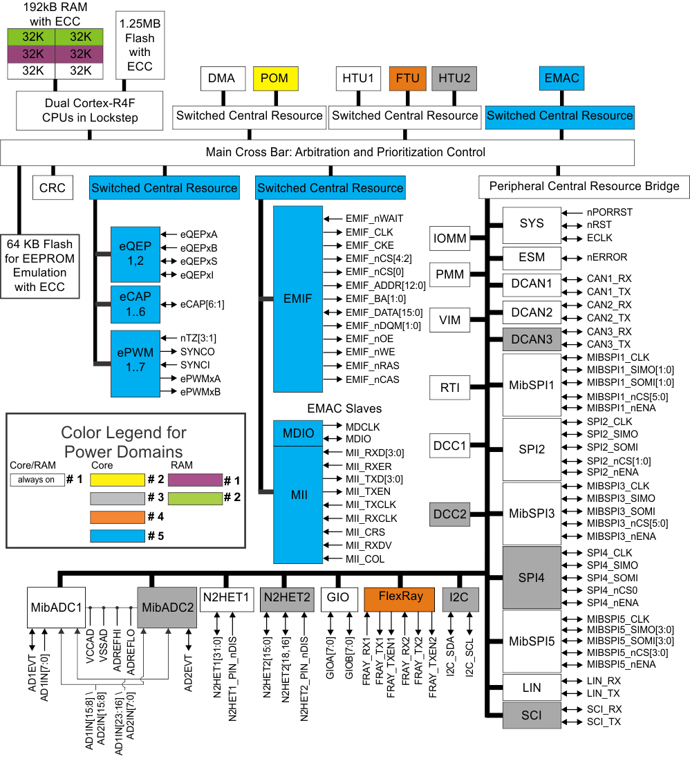
The TMS570LS1227
device
is a high-performance
automotive-grade microcontroller family for safety systems. The safety architecture includes
dual CPUs in lockstep, CPU and memory BIST logic, ECC on both the flash and the data SRAM, parity
on peripheral memories, and loopback capability on peripheral I/Os.The TMS570LS1227
device
integrates the ARM Cortex-R4F
floating-point
CPU which offers an efficient 1.66 DMIPS/MHz, and
has configurations which
can run up to 180 MHz providing
up to 298 DMIPS.
The
device supports the word-invariant big-endian [BE32] format.The TMS570LS1227
device
has 1.25MB of integrated
flash and 192KB of data RAM with single-bit error correction and
double-bit error detection. The flash memory on this device is a
nonvolatile, electrically erasable and
programmable memory, implemented with a 64-bit-wide data bus
interface. The flash operates on a
3.3-V supply input (same level as I/O supply) for all read, program,
and erase operations. When in
pipeline mode, the flash operates with a system clock frequency of
up to 180 MHz. The SRAM
supports single-cycle read and write accesses in byte, halfword,
word, and double-word modes
throughout the supported frequency range.The TMS570LS1227
device
features peripherals for real-time control-based applications, including
two Next Generation High-End Timer (N2HET) timing
coprocessors
with up to 44 I/O terminals, seven Enhanced Pulse Width Modulator (ePWM) modules with up to 14
outputs, six Enhanced Capture (eCAP) modules, two Enhanced Quadrature Encoder Pulse (eQEP) modules,
and two 12-bit Analog-to-Digital Converters (ADCs) supporting up to 24 inputs.The N2HET is an advanced intelligent timer that provides sophisticated timing functions
for real-time applications. The timer is software-controlled, using a reduced instruction set, with
a specialized timer micromachine and an attached I/O port. The N2HET can be used for
pulse-width-modulated outputs, capture or compare inputs, or general-purpose I/O (GIO). The N2HET
is especially well suited for applications requiring multiple sensor information and drive
actuators with complex and accurate time pulses. A High-End Timer Transfer Unit (HTU) can perform
DMA-type transactions to transfer N2HET data to or from main memory. A Memory Protection Unit (MPU)
is built into the HTU.The
ePWM module can generate complex pulse width waveforms with minimal CPU overhead or intervention.
The ePWM is easy to use and it supports both high-side and low-side PWM and deadband generation.
With integrated trip zone protection and synchronization with the on-chip MibADC, the ePWM module
is ideal for digital motor control applications.The
eCAP module is essential in systems where the accurately timed capture of external events is
important. The eCAP can also be used to monitor the ePWM outputs or for simple PWM generation when
the eCAP is not needed for capture applications.The
eQEP module is used for direct interface with a linear or rotary incremental encoder to get
position, direction, and speed information from a rotating machine as used in high-performance
motion and position-control systems.The device has
two
12-bit-resolution
MibADCs with
24 total inputs and 64 words
of parity-protected buffer RAM each. The MibADC channels can be converted individually or can be
grouped by software for sequential conversion sequences.
Sixteen
inputs are shared between the two MibADCs. Each MibADC supports three separate groupings of
channels. Each group can be converted once when triggered or configured for continuous conversion
mode.
The MibADC has a 10-bit mode for use when compatibility with older devices or faster conversion
time is desired.
MibADC1 also supports the use of external analog multiplexers.The device has multiple communication interfaces:
three MibSPIs,
two
SPIs, one LIN,
one
SCI, three DCANs,
one I2C,
one Ethernet, and one FlexRay controller
with two channels. The SPI
provides a convenient method of serial high-speed communications
between similar shift-register
type devices. The LIN supports the Local Interconnect standard 2.0
and can be used as a UART in
full-duplex mode using the standard Non-Return-to-Zero (NRZ) format.
The DCAN supports the CAN 2.0
(A and B) protocol standard and uses a serial, multimaster
communication protocol that efficiently
supports distributed real-time control with robust communication
rates of up to 1 Mbps. The DCAN is
ideal for systems operating in noisy and harsh environments (for
example, automotive and industrial
fields) that require reliable serial communication or multiplexed
wiring. The FlexRay controller uses
a dual-channel serial, fixed time base multimaster communication
protocol with communication rates
of 10 Mbps per channel. A FlexRay Transfer Unit (FTU) enables
autonomous transfers of FlexRay data
to and from main CPU memory. Transfers are protected by a dedicated,
built-in MPU. The Ethernet module supports MII, RMII, and
MDIO interfaces. The
I2C module is a multimaster communication module providing an interface between the microcontroller
and an I2C-compatible device through the I2C
serial bus. The I2C supports speeds of 100 and 400 Kbps.A Frequency-Modulated Phase-Locked Loop (FMPLL) clock module is used to multiply the
external frequency reference to a higher frequency for internal use.
The Global Clock Module (GCM) manages the mapping between the available clock sources and the
device clock domains.The device also has an External Clock Prescaler (ECP) module that when enabled, outputs
a continuous external clock on the ECLK terminal. The ECLK frequency is a user-programmable ratio
of the peripheral interface clock (VCLK) frequency. This low-frequency output can be monitored
externally as an indicator of the device operating frequency.The Direct Memory Access (DMA) controller has 16 channels, 32 control packets, and
parity protection on its memory. An MPU is built into the DMA to protect memory against erroneous
transfers.The Error Signaling Module (ESM) monitors all device errors and determines whether an
interrupt or external error pin (ball) is triggered when a fault is detected. The nERROR terminal
can be monitored externally as an indicator of a fault condition in the microcontroller.The
External Memory Interface (EMIF) provides a memory extension to asynchronous and synchronous
memories or other slave devices.A
Parameter Overlay Module (POM) enhances the calibration capabilities of application code. The POM
can reroute flash accesses to internal memory or to the EMIF, thus avoiding the reprogramming steps
necessary for parameter updates in flash.With integrated safety features and a wide choice of communication and control
peripherals, the TMS570LS1227
device
is an ideal solution for high-performance real-time control applications with safety-critical
requirements.
TMS5701227CPGEQQ1 电路图
TMS5701227CPGEQQ1 电路图
TMS5701227CPGEQQ1 相关产品
- 14305R-2000
- 3530ECUSAGRM
- 5CEBA2F23C8N
- 5CEBA2U15C6N
- 5CEBA2U15C8N
- 5CEBA2U15I7N
- 5CEBA2U19C8N
- 5CEBA4U15C7N
- 5CEBA4U15C8N
- 5CEBA4U19C7N
- 5CEBA5U19C8N
- 5CEBA7F31C8N
- 5CEBA9F23C7N
- 5CEBA9F23C8N
- 5CEBA9F31C7N
- 5CEFA2F23C6N
- 5CEFA4F23C7N
- 5CEFA4F23I7N
- 5CEFA4U19C6N
- 5CEFA4U19C8N
- 5CEFA5F23C6N
- 5CEFA5F23I7N
- 5CEFA5U19C7N
- 5CEFA7F23C6N
- 5CEFA7F23C7N
- 5CEFA7F27I7N
- 5CEFA7F31C7N
- 5CEFA7F31I7N
- 5CEFA7U19A7N
- 5CEFA9F23C7N