 搜索
搜索
 发布采购
发布采购
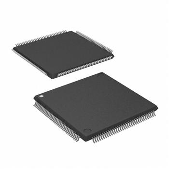
- 封装:144-LQFP
- RoHS:无铅 / 符合限制有害物质指令(RoHS)规范要求
- 包装方式:托盘
- 参考价格:$10.24-$9.92
更新日期:2024-04-01 00:04:00
产品简介:数字信号处理器
查看详情- 封装:144-LQFP
- RoHS:无铅 / 符合限制有害物质指令(RoHS)规范要求
- 包装方式:托盘
- 参考价格:$10.24-$9.92
TMS320VC5404PGE 供应商
- 公司
- 型号
- 品牌
- 封装/批号
- 数量
- 地区
- 日期
- 说明
- 询价
-
TI
-
原厂原装
22+ -
3288
-
上海市
-
-
-
一级代理原装
-
TI
-
-
2019+ -
5800
-
上海市
-
-
-
全新原装现货
-
TI(德州仪器)
-
LQFP-144(20x20)
2022+ -
12000
-
上海市
-
-
-
原装可开发票
-
TI
-
-
21+ -
5000
-
上海市
-
-
-
原装现货,品质为先,请来电垂询!
-
TI
-
原厂原装
2318+ -
9200
-
合肥
-
-
-
科大讯飞战略投资企业
TMS320VC5404PGE 中文资料属性参数
- 标准包装:60
- 类别:集成电路 (IC)
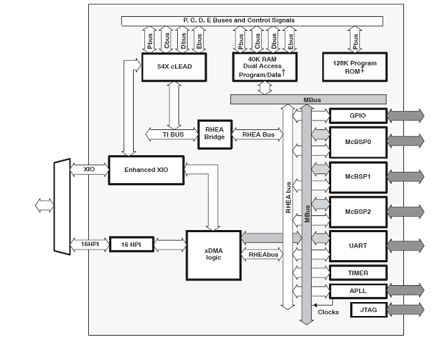
- 家庭:嵌入式 - DSP(数字式信号处理器)
- 系列:TMS320C54x
- 类型:定点
- 接口:主机接口,McBSP,UART
- 时钟速率:120MHz
- 非易失内存:ROM(128 kB)
- 芯片上RAM:32kB
- 电压 - 输入/输出:3.30V
- 电压 - 核心:1.50V
- 工作温度:0°C ~ 100°C
- 安装类型:表面贴装
- 封装/外壳:144-LQFP
- 供应商设备封装:144-LQFP(20x20)
- 包装:托盘
- 配用:296-15829-ND - DSP STARTER KIT FOR TMS320C5416
- 其它名称:296-15712
产品特性
- Advanced Multibus Architecture With Three Separate 16-Bit Data Memory Buses and One Program Memory Bus
- 40-Bit Arithmetic Logic Unit (ALU) Including a 40-Bit Barrel Shifter and Two Independent 40-Bit Accumulators
- 17- × 17-Bit Parallel Multiplier Coupled to a 40-Bit Dedicated Adder for Non-Pipelined Single-Cycle Multiply/Accumulate (MAC) Operation
- Compare, Select, and Store Unit (CSSU) for the Add/Compare Selection of the Viterbi Operator
- Exponent Encoder to Compute an Exponent Value of a 40-Bit Accumulator Value in a Single Cycle
- Two Address Generators With Eight Auxiliary Registers and Two Auxiliary Register Arithmetic Units (ARAUs)
- Data Bus With a Bus Holder Feature
- Extended Addressing Mode for 8M × 16-Bit Maximum Addressable External Program Space
- On-Chip ROM 128K × 16-Bit (5407) Configured for Program Memory 64K × 16-Bit (5404) Configured for Program Memory
- 128K × 16-Bit (5407) Configured for Program Memory
- 64K × 16-Bit (5404) Configured for Program Memory
- On-Chip RAM 40K × 16-Bit (5407) Composed of Five Blocks of 8K × 16-Bit On-Chip Dual-Access Program/Data RAM 16K x 16-Bit (5404) Composed of Two Blocks of 8K × 16-Bit On-Chip Dual-Access Program/Data RAM
- 40K × 16-Bit (5407) Composed of Five Blocks of 8K × 16-Bit On-Chip Dual-Access Program/Data RAM
- 16K x 16-Bit (5404) Composed of Two Blocks of 8K × 16-Bit On-Chip Dual-Access Program/Data RAM
- Enhanced External Parallel Interface (XIO2)
- Single-Instruction-Repeat and Block-Repeat Operations for Program Code
- Block-Memory-Move Instructions for Better Program and Data Management
- Instructions With a 32-Bit Long Word Operand
- Instructions With Two- or Three-Operand Reads
- Arithmetic Instructions With Parallel Store and Parallel Load
- Conditional Store Instructions
- Fast Return From Interrupt
- On-Chip Peripherals Software-Programmable Wait-State Generator and Programmable Bank-Switching On-Chip Programmable Phase-Locked Loop (PLL) Clock Generator With External Clock Source Two 16-Bit Timers Six-Channel Direct Memory Access (DMA) Controller Three Multichannel Buffered Serial Ports (McBSPs) 8/16-Bit Enhanced Parallel Host-Port Interface (HPI8/16) Universal Asynchronous Receiver/Transmitter (UART) With Integrated Baud Rate Generator
- Software-Programmable Wait-State Generator and Programmable Bank-Switching
- On-Chip Programmable Phase-Locked Loop (PLL) Clock Generator With External Clock Source
- Two 16-Bit Timers
- Six-Channel Direct Memory Access (DMA) Controller
- Three Multichannel Buffered Serial Ports (McBSPs)
- 8/16-Bit Enhanced Parallel Host-Port Interface (HPI8/16)
- Universal Asynchronous Receiver/Transmitter (UART) With Integrated Baud Rate Generator
- Power Consumption Control With IDLE1, IDLE2, and IDLE3 Instructions With Power-Down Modes
- CLKOUT Off Control to Disable CLKOUT
- On-Chip Scan-Based Emulation Logic, IEEE Std 1149.1 (JTAG) Boundary Scan Logic
- 144-Pin Ball Grid Array (BGA) (GGU Suffix)
- 144-Pin Low-Profile Quad Flatpack (LQFP) (PGE Suffix)
- 8.33-ns Single-Cycle Fixed-Point Instruction Execution Time (120 MIPS)
- 3.3-V I/O Supply Voltage
- 1.5-V Core Supply Voltage
产品概述
This data manual discusses features and specifications of the TMS320VC5407 and TMS320VC5404 (hereafter referred to as the 5407/5404 unless otherwise specified) digital signal processors (DSPs). The 5407 and 5404 are essentially the same device except for differences in their memory maps.This section lists the pin assignments and describes the function of each pin. This data manual also provides a detailed description section, electrical specifications, parameter measurement information, and mechanical data about the available packaging.NOTE: This data sheet is designed to be used in conjunction with the TMS320C5000 DSP Family Functional Overview (literature number SPRU307).The 5407/5404 are based on an advanced modified Harvard architecture that has one program memory bus and three data memory buses. These processors provide an arithmetic logic unit (ALU) with a high degree of parallelism, application-specific hardware logic, on-chip memory, and additional on-chip peripherals. The basis of the operational flexibility and speed of these DSPs is a highly specialized instruction set.Separate program and data spaces allow simultaneous access to program instructions and data, providing a high degree of parallelism. Two read operations and one write operation can be performed in a single cycle. Instructions with parallel store and application-specific instructions can fully utilize this architecture. In addition, data can be transferred between data and program spaces. Such parallelism supports a powerful set of arithmetic, logic, and bit-manipulation operations that can all be performed in a single machine cycle. These DSPs also include the control mechanisms to manage interrupts, repeated operations, and function calls.
TMS320VC5404PGE 数据手册
| 数据手册 | 说明 | 数量 | 操作 |
|---|---|---|---|
 TMS320VC5404PGE TMS320VC5404PGE
|
Fixed-Point Digital Signal Processors |
110 Pages页,1.32M | 查看 |
TMS320VC5404PGE 电路图
TMS320VC5404PGE 电路图
TMS320VC5404PGE 相关产品
- ADSP-2104BPZ-80
- ADSP-2105BPZ-80
- ADSP-21060CZ-160
- ADSP-21060KBZ-160
- ADSP-21060KSZ-133
- ADSP-21060LABZ-160
- ADSP-21060LCB-133
- ADSP-21060LCW-160
- ADSP-21060LKSZ-133
- ADSP-21061LASZ-176
- ADSP-21061LKSZ-176
- ADSP-21062KBZ-160
- ADSP-21062KSZ-160
- ADSP-21062LCSZ-160
- ADSP-21062LKBZ-160
- ADSP-21065LCCAZ240
- ADSP-21065LKCAZ264
- ADSP-21160NCB-100
- ADSP-21160NCBZ-100
- ADSP-21160NKBZ-100
- ADSP-21161NKCAZ100
- ADSP-21261SKSTZ150
- ADSP-21262SBBC-150
- ADSP-21262SBBCZ150
- ADSP-21266SKBCZ-2D
- ADSP-21266SKSTZ-1D
- ADSP-21266SKSTZ-2D
- ADSP-21362BSWZ-1AA
- ADSP-21363BBC-1AA
- ADSP-21363YSWZ-2AA