 搜索
搜索
 发布采购
发布采购
更新日期:2024-04-01 00:04:00

产品简介:低功耗 C674x 浮点 DSP- 456MHz、PBGA
查看详情TMS320C6747DZKB4 供应商
- 公司
- 型号
- 品牌
- 封装/批号
- 数量
- 地区
- 日期
- 说明
- 询价
-
TI
-
原厂原装
22+ -
3288
-
上海市
-
-
-
一级代理原装
-
TI
-
原厂原装
2318+ -
9200
-
合肥
-
-
-
科大讯飞战略投资企业
TMS320C6747DZKB4 中文资料属性参数
- 现有数量:0现货查看交期
- 价格:1 : ¥165.28000托盘
- 系列:TMS320C674x
- 包装:托盘
- 产品状态:在售
- 类型:定点/浮点
- 接口:EBI/EMI,以太网 MAC,主机接口,I2C,McASP,SPI,UART,USB
- 时钟速率:456MHz
- 非易失性存储器:外部
- 片载 RAM:448kB
- 电压 - I/O:3.30V
- 电压 - 内核:1.20V
- 工作温度:0°C ~ 90°C(TJ)
- 安装类型:表面贴装型
- 封装/外壳:256-BGA
- 供应商器件封装:256-BGA(17x17)
产品特性
- Software Support TI DSP/BIOS™ Chip Support Library and DSP Library
- TI DSP/BIOS™
- Chip Support Library and DSP Library
- 375- and 456-MHz TMS320C674x VLIW DSP
- C674x Instruction Set Features Superset of the C67x+ and C64x+ ISAs Up to 3648 MIPS and 2736 MFLOPS C674x Byte-Addressable (8-, 16-, 32-, and 64-Bit Data) 8-Bit Overflow Protection Bit-Field Extract, Set, Clear Normalization, Saturation, Bit-Counting Compact 16-Bit Instructions
- Superset of the C67x+ and C64x+ ISAs
- Up to 3648 MIPS and 2736 MFLOPS C674x
- Byte-Addressable (8-, 16-, 32-, and 64-Bit Data)
- 8-Bit Overflow Protection
- Bit-Field Extract, Set, Clear
- Normalization, Saturation, Bit-Counting
- Compact 16-Bit Instructions
- C674x Two-Level Cache Memory Architecture 32KB of L1P Program RAM/Cache 32KB of L1D Data RAM/Cache 256KB of L2 Unified Mapped RAM/Cache Flexible RAM/Cache Partition (L1 and L2)
- 32KB of L1P Program RAM/Cache
- 32KB of L1D Data RAM/Cache
- 256KB of L2 Unified Mapped RAM/Cache
- Flexible RAM/Cache Partition (L1 and L2)
- Enhanced Direct Memory Access Controller 3 (EDMA3): 2 Transfer Controllers 32 Independent DMA Channels 8 Quick DMA Channels Programmable Transfer Burst Size
- 2 Transfer Controllers
- 32 Independent DMA Channels
- 8 Quick DMA Channels
- Programmable Transfer Burst Size
- TMS320C674x Fixed- and Floating-Point VLIW DSP Core Load-Store Architecture with Nonaligned Support 64 General-Purpose Registers (32-Bit) Six ALU (32- and 40-Bit) Functional Units Supports 32-Bit Integer, SP (IEEE Single Precision/32-Bit) and DP (IEEE Double Precision/64-Bit) Floating Point Supports up to Four SP Additions Per Clock, Four DP Additions Every 2 Clocks Supports up to Two Floating-Point (SP or DP) Reciprocal Approximation (RCPxP) and Square-Root Reciprocal Approximation (RSQRxP) Operations Per Cycle Two Multiply Functional Units Mixed-Precision IEEE Floating Point Multiply Supported up to: 2 SP x SP -> SP Per Clock 2 SP x SP -> DP Every Two Clocks 2 SP x DP -> DP Every Three Clocks 2 DP x DP -> DP Every Four Clocks Fixed-Point Multiply Supports Two 32 x 32-Bit Multiplies, Four 16 x 16-Bit Multiplies, or Eight 8 x 8-Bit Multiplies per Clock Cycle, and Complex Multiples Instruction Packing Reduces Code Size All Instructions Conditional Hardware Support for Modulo Loop Operation Protected Mode Operation Exceptions Support for Error Detection and Program Redirection
- Load-Store Architecture with Nonaligned Support
- 64 General-Purpose Registers (32-Bit)
- Six ALU (32- and 40-Bit) Functional Units Supports 32-Bit Integer, SP (IEEE Single Precision/32-Bit) and DP (IEEE Double Precision/64-Bit) Floating Point Supports up to Four SP Additions Per Clock, Four DP Additions Every 2 Clocks Supports up to Two Floating-Point (SP or DP) Reciprocal Approximation (RCPxP) and Square-Root Reciprocal Approximation (RSQRxP) Operations Per Cycle
- Supports 32-Bit Integer, SP (IEEE Single Precision/32-Bit) and DP (IEEE Double Precision/64-Bit) Floating Point
- Supports up to Four SP Additions Per Clock, Four DP Additions Every 2 Clocks
- Supports up to Two Floating-Point (SP or DP) Reciprocal Approximation (RCPxP) and Square-Root Reciprocal Approximation (RSQRxP) Operations Per Cycle
- Two Multiply Functional Units Mixed-Precision IEEE Floating Point Multiply Supported up to: 2 SP x SP -> SP Per Clock 2 SP x SP -> DP Every Two Clocks 2 SP x DP -> DP Every Three Clocks 2 DP x DP -> DP Every Four Clocks Fixed-Point Multiply Supports Two 32 x 32-Bit Multiplies, Four 16 x 16-Bit Multiplies, or Eight 8 x 8-Bit Multiplies per Clock Cycle, and Complex Multiples
- Mixed-Precision IEEE Floating Point Multiply Supported up to: 2 SP x SP -> SP Per Clock 2 SP x SP -> DP Every Two Clocks 2 SP x DP -> DP Every Three Clocks 2 DP x DP -> DP Every Four Clocks
- 2 SP x SP -> SP Per Clock
- 2 SP x SP -> DP Every Two Clocks
- 2 SP x DP -> DP Every Three Clocks
- 2 DP x DP -> DP Every Four Clocks
- Fixed-Point Multiply Supports Two 32 x 32-Bit Multiplies, Four 16 x 16-Bit Multiplies, or Eight 8 x 8-Bit Multiplies per Clock Cycle, and Complex Multiples
- Instruction Packing Reduces Code Size
- All Instructions Conditional
- Hardware Support for Modulo Loop Operation
- Protected Mode Operation
- Exceptions Support for Error Detection and Program Redirection
- 128KB of RAM Shared Memory (TMS320C6747 Only)
- 3.3-V LVCMOS I/Os (Except for USB Interfaces)
- Two External Memory Interfaces: EMIFA NOR (8- or 16-Bit-Wide Data) NAND (8- or 16-Bit-Wide Data) 16-Bit SDRAM with 128-MB Address Space (TMS320C6747 Only) EMIFB 32-Bit or 16-Bit SDRAM with 256-MB Address Space (TMS320C6747) 16-Bit SDRAM with 128-MB Address Space (TMS320C6745)
- EMIFA NOR (8- or 16-Bit-Wide Data) NAND (8- or 16-Bit-Wide Data) 16-Bit SDRAM with 128-MB Address Space (TMS320C6747 Only)
- NOR (8- or 16-Bit-Wide Data)
- NAND (8- or 16-Bit-Wide Data)
- 16-Bit SDRAM with 128-MB Address Space (TMS320C6747 Only)
- EMIFB 32-Bit or 16-Bit SDRAM with 256-MB Address Space (TMS320C6747) 16-Bit SDRAM with 128-MB Address Space (TMS320C6745)
- 32-Bit or 16-Bit SDRAM with 256-MB Address Space (TMS320C6747)
- 16-Bit SDRAM with 128-MB Address Space (TMS320C6745)
- Three Configurable 16550-Type UART Modules: UART0 with Modem Control SignalsAutoflow Control Signals (CTS, RTS) on UART0 Only 16-Byte FIFO 16x or 13x Oversampling Option
- UART0 with Modem Control Signals
- Autoflow Control Signals (CTS, RTS) on UART0 Only
- 16-Byte FIFO
- 16x or 13x Oversampling Option
- LCD Controller (TMS320C6747 Only)
- Two Serial Peripheral Interfaces (SPIs) Each with One Chip Select
- Multimedia Card (MMC)/Secure Digital (SD) Card Interface with Secure Data I/O (SDIO)
- Two Master and Slave Inter-Integrated Circuit (I2C Bus™)
- One Host-Port Interface (HPI) with 16-Bit-Wide Muxed Address/Data Bus for High Bandwidth (TMS320C6747 Only)
- Programmable Real-Time Unit Subsystem (PRUSS) Two Independent Programmable Realtime Unit (PRU) Cores 32-Bit Load and Store RISC Architecture 4KB of Instruction RAM per Core 512 Bytes of Data RAM per Core PRUSS can be Disabled via Software to Save Power Standard Power-Management Mechanism Clock Gating Entire Subsystem Under a Single PSC Clock Gating Domain Dedicated Interrupt Controller Dedicated Switched Central Resource
- Two Independent Programmable Realtime Unit (PRU) Cores 32-Bit Load and Store RISC Architecture 4KB of Instruction RAM per Core 512 Bytes of Data RAM per Core PRUSS can be Disabled via Software to Save Power
- 32-Bit Load and Store RISC Architecture
- 4KB of Instruction RAM per Core
- 512 Bytes of Data RAM per Core
- PRUSS can be Disabled via Software to Save Power
- Standard Power-Management Mechanism Clock Gating Entire Subsystem Under a Single PSC Clock Gating Domain
- Clock Gating
- Entire Subsystem Under a Single PSC Clock Gating Domain
- Dedicated Interrupt Controller
- Dedicated Switched Central Resource
- USB 1.1 OHCI (Host) with Integrated PHY (USB1) (TMS320C6747 Only)
- USB 2.0 OTG Port with Integrated PHY (USB0) USB 2.0 High- and Full-Speed Client (TMS320C6747) USB 2.0 Full-Speed Client (TMS320C6745) USB 2.0 High-, Full-, and Low-Speed Host (TMS320C6747) USB 2.0 Full- and Low-Speed Host (TMS320C6745) High-Speed Functionality Available on TMS320C6747 Device Only End Point 0 (Control) End Points 1,2,3,4 (Control, Bulk, Interrupt or ISOC) RX and TX
- USB 2.0 High- and Full-Speed Client (TMS320C6747)
- USB 2.0 Full-Speed Client (TMS320C6745)
- USB 2.0 High-, Full-, and Low-Speed Host (TMS320C6747)
- USB 2.0 Full- and Low-Speed Host (TMS320C6745)
- High-Speed Functionality Available on TMS320C6747 Device Only
- End Point 0 (Control)
- End Points 1,2,3,4 (Control, Bulk, Interrupt or ISOC) RX and TX
- Three Multichannel Audio Serial Ports (McASPs): TMS320C6747 Supports 3 McASPsTMS320C6745 Supports 2 McASPs Six Clock Zones and 28 Serial Data Pins Supports TDM, I2S, and Similar Formats DIT-Capable (McASP2) FIFO Buffers for Transmit and Receive
- TMS320C6747 Supports 3 McASPs
- TMS320C6745 Supports 2 McASPs
- Six Clock Zones and 28 Serial Data Pins
- Supports TDM, I2S, and Similar Formats
- DIT-Capable (McASP2)
- FIFO Buffers for Transmit and Receive
- 10/100 Mbps Ethernet MAC (EMAC): IEEE 802.3 Compliant (3.3-V I/O Only) RMII Media-Independent Interface Management Data I/O (MDIO) Module
- IEEE 802.3 Compliant (3.3-V I/O Only)
- RMII Media-Independent Interface
- Management Data I/O (MDIO) Module
- Real-Time Clock with 32-kHz Oscillator and Separate Power Rail (TMS320C6747 Only)
- One 64-Bit General-Purpose Timer (Configurable as Two 32-Bit Timers)
- One 64-Bit General-Purpose Watchdog Timer (Configurable as Two 32-Bit General-Purpose Timers)
- Three Enhanced Pulse Width Modulators (eHRPWMs): Dedicated 16-Bit Time-Base Counter with Period and Frequency Control 6 Single Edge, 6 Dual Edge Symmetric, or 3 Dual Edge Asymmetric Outputs Dead-Band Generation PWM Chopping by High-Frequency Carrier Trip Zone Input
- Dedicated 16-Bit Time-Base Counter with Period and Frequency Control
- 6 Single Edge, 6 Dual Edge Symmetric, or 3 Dual Edge Asymmetric Outputs
- Dead-Band Generation
- PWM Chopping by High-Frequency Carrier
- Trip Zone Input
- Three 32-Bit Enhanced Capture (eCAP) Modules: Configurable as 3 Capture Inputs or 3 Auxiliary Pulse Width Modulator (APWM) Outputs Single-Shot Capture of up to Four Event Time-Stamps
- Configurable as 3 Capture Inputs or 3 Auxiliary Pulse Width Modulator (APWM) Outputs
- Single-Shot Capture of up to Four Event Time-Stamps
- Two 32-Bit Enhanced Quadrature Encoder Pulse (eQEP) Modules
- TMS320C6747 Device: 256-Ball Pb-Free Plastic Ball Grid Array (PBGA) [ZKB Suffix], 1.0-mm Ball Pitch
- 256-Ball Pb-Free Plastic Ball Grid Array (PBGA) [ZKB Suffix], 1.0-mm Ball Pitch
- TMS320C6745 Device: 176-pin PowerPAD™ Plastic Quad Flat Pack [PTP suffix], 0.5-mm Pin Pitch
- 176-pin PowerPAD™ Plastic Quad Flat Pack [PTP suffix], 0.5-mm Pin Pitch
- Commercial, Industrial, Extended, or Automotive Temperature
产品概述
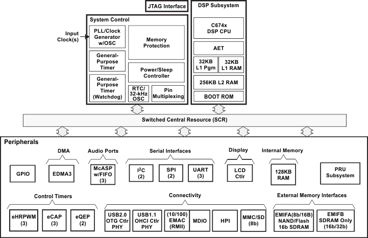
The TMS320C6745/6747 device is a low-power digital signal processor based on
a TMS320C674x DSP core. It consumes significantly
lower power than other members of the TMS320C6000™
platform of DSPs.The TMS320C6745/6747 device enables original-equipment manufacturers (OEMs) and
original-design manufacturers (ODMs) to quickly bring to market devices featuring
high
processing performance .The TMS320C6745/6747 DSP core uses a two-level cache-based architecture. The
Level 1 program cache (L1P) is a 32-KB direct mapped cache and the Level 1 data cache (L1D) is a
32-KB 2-way set-associative cache. The Level 2 program cache (L2P) consists of a 256-KB memory
space that is shared between program and data space. L2 memory can be configured as mapped memory,
cache, or combinations of the two. Although the DSP L2 is accessible by other hosts in the system, an additional 128KB of RAM shared memory
(TMS320C6747 only) is available for use by other hosts without
affecting DSP performance. The peripheral set includes: a 10/100 Mbps Ethernet MAC (EMAC) with a management data
input/output (MDIO) module; two I2C Bus interfaces; 3 multichannel audio
serial ports (McASPs) with 16/9
serializers and FIFO buffers; two 64-bit general-purpose timers each configurable (one configurable
as watchdog); a configurable 16-bit host-port interface (HPI) [TMS320C6747
only]; up to 8 banks of 16 pins of general-purpose input/output (GPIO) with programmable
interrupt/event generation modes, multiplexed with other peripherals; 3 UART interfaces (one with
both RTS and CTS); three enhanced high-resolution
pulse width modulator (eHRPWM) peripherals; three 32-bit enhanced capture (eCAP) module peripherals
which can be configured as 3 capture inputs or 3 auxiliary pulse width modulator (APWM) outputs;
two 32-bit enhanced quadrature encoded pulse (eQEP) peripherals; and 2 external memory interfaces:
an asynchronous and SDRAM external memory interface (EMIFA) for slower memories or peripherals, and
a higher speed memory interface (EMIFB) for SDRAM.The Ethernet Media Access Controller (EMAC) provides an efficient interface between the
TMS320C6745/6747 device and
the network. The EMAC supports both 10Base-T and 100Base-TX, or 10 Mbps and 100 Mbps in either
half- or full-duplex mode. Additionally, an MDIO interface is available for PHY configuration.
The rich peripheral set provides the ability to control external peripheral devices
and communicate with external processors. For details on each of the peripherals, see the related
sections later in this document and the associated peripheral reference guides.
TMS320C6747DZKB4 电路图
TMS320C6747DZKB4 电路图
TMS320C6747DZKB4 相关产品
- 14305R-2000
- 3530ECUSAGRM
- 5CEBA2F23C8N
- 5CEBA2U15C6N
- 5CEBA2U15C8N
- 5CEBA2U15I7N
- 5CEBA2U19C8N
- 5CEBA4U15C7N
- 5CEBA4U15C8N
- 5CEBA4U19C7N
- 5CEBA5U19C8N
- 5CEBA7F31C8N
- 5CEBA9F23C7N
- 5CEBA9F23C8N
- 5CEBA9F31C7N
- 5CEFA2F23C6N
- 5CEFA4F23C7N
- 5CEFA4F23I7N
- 5CEFA4U19C6N
- 5CEFA4U19C8N
- 5CEFA5F23C6N
- 5CEFA5F23I7N
- 5CEFA5U19C7N
- 5CEFA7F23C6N
- 5CEFA7F23C7N
- 5CEFA7F27I7N
- 5CEFA7F31C7N
- 5CEFA7F31I7N
- 5CEFA7U19A7N
- 5CEFA9F23C7N