 搜索
搜索
 发布采购
发布采购
- 封装:272-BBGA
- RoHS:无铅 / 符合限制有害物质指令(RoHS)规范要求
- 包装方式:托盘
- 参考价格:$18-$30
更新日期:2024-04-01 00:04:00

产品简介:C67x 浮点 DSP- 高达 250MHz、McBSP、32 位 EMIFA
查看详情- 封装:272-BBGA
- RoHS:无铅 / 符合限制有害物质指令(RoHS)规范要求
- 包装方式:托盘
- 参考价格:$18-$30
TMS320C6711DZDP200 供应商
- 公司
- 型号
- 品牌
- 封装/批号
- 数量
- 地区
- 日期
- 说明
- 询价
-
TI
-
原厂原装
22+ -
3288
-
上海市
-
-
-
一级代理原装
-
TI(德州仪器)
-
BGA-272
2022+ -
12000
-
上海市
-
-
-
原装可开发票
-
TI
-
数字信号处理器与控制器
21+ -
1080
-
上海市
-
-
-
原装现货,品质为先,请来电垂询!
-
TI
-
原厂原装
2318+ -
9200
-
合肥
-
-
-
科大讯飞战略投资企业
TMS320C6711DZDP200 中文资料属性参数
- 标准包装:40
- 类别:集成电路 (IC)
- 家庭:嵌入式 - DSP(数字式信号处理器)
- 系列:TMS320C67x
- 类型:浮点
- 接口:主机接口,McBSP
- 时钟速率:200MHz
- 非易失内存:外部
- 芯片上RAM:72kB
- 电压 - 输入/输出:3.30V
- 电压 - 核心:1.26V
- 工作温度:0°C ~ 90°C
- 安装类型:表面贴装
- 封装/外壳:272-BBGA
- 供应商设备封装:272-BGA(27x27)
- 包装:托盘
- 配用:TMDX320036711-ND - DEVELOPMENT KIT TCPP/IP NETWORK
- 其它名称:296-19389
产品特性
- Excellent-Price/Performance Floating-Point Digital Signal Processor (DSP): TMS320C6711D Eight 32-Bit Instructions/Cycle 167-, 200-, 250-MHz Clock Rates 6-, 5-, 4-ns Instruction Cycle Time 1000, 1200, 1500 MFLOPS
- Eight 32-Bit Instructions/Cycle
- 167-, 200-, 250-MHz Clock Rates
- 6-, 5-, 4-ns Instruction Cycle Time
- 1000, 1200, 1500 MFLOPS
- Advanced Very Long Instruction Word (VLIW) C67x™ DSP Core Eight Highly Independent Functional Units: Four ALUs (Floating- and Fixed-Point) Two ALUs (Fixed-Point) Two Multipliers (Floating- and Fixed-Point) Load-Store Architecture With 32 32-Bit General-Purpose Registers Instruction Packing Reduces Code Size All Instructions Conditional
- Eight Highly Independent Functional Units: Four ALUs (Floating- and Fixed-Point) Two ALUs (Fixed-Point) Two Multipliers (Floating- and Fixed-Point)
- Four ALUs (Floating- and Fixed-Point)
- Two ALUs (Fixed-Point)
- Two Multipliers (Floating- and Fixed-Point)
- Load-Store Architecture With 32 32-Bit General-Purpose Registers
- Instruction Packing Reduces Code Size
- All Instructions Conditional
- Instruction Set Features Hardware Support for IEEE Single-Precision and Double-Precision Instructions Byte-Addressable (8-, 16-, 32-Bit Data) 8-Bit Overflow Protection Saturation Bit-Field Extract, Set, Clear Bit-Counting Normalization
- Hardware Support for IEEE Single-Precision and Double-Precision Instructions
- Byte-Addressable (8-, 16-, 32-Bit Data)
- 8-Bit Overflow Protection
- Saturation
- Bit-Field Extract, Set, Clear
- Bit-Counting
- Normalization
- L1/L2 Memory Architecture 32K-Bit (4K-Byte) L1P Program Cache (Direct Mapped) 32K-Bit (4K-Byte) L1D Data Cache (2-Way Set-Associative) 512K-Bit (64K-Byte) L2 Unified Mapped RAM/Cache (Flexible Data/Program Allocation)
- 32K-Bit (4K-Byte) L1P Program Cache (Direct Mapped)
- 32K-Bit (4K-Byte) L1D Data Cache (2-Way Set-Associative)
- 512K-Bit (64K-Byte) L2 Unified Mapped RAM/Cache (Flexible Data/Program Allocation)
- Device Configuration Boot Mode: HPI, 8-, 16-, 32-Bit ROM Boot Endianness: Little Endian, Big Endian
- Boot Mode: HPI, 8-, 16-, 32-Bit ROM Boot
- Endianness: Little Endian, Big Endian
- Enhanced Direct-Memory-Access (EDMA) Controller (16 Independent Channels)
- 32-Bit External Memory Interface (EMIF) Glueless Interface to Asynchronous Memories: SRAM and EPROM Glueless Interface to Synchronous Memories: SDRAM and SBSRAM 256M-Byte Total Addressable External Memory Space
- Glueless Interface to Asynchronous Memories: SRAM and EPROM
- Glueless Interface to Synchronous Memories: SDRAM and SBSRAM
- 256M-Byte Total Addressable External Memory Space
- 16-Bit Host-Port Interface (HPI)
- Two Multichannel Buffered Serial Ports (McBSPs) Direct Interface to T1/E1, MVIP, SCSA Framers ST-Bus-Switching Compatible Up to 256 Channels Each AC97-Compatible Serial-Peripheral-Interface (SPI) Compatible (Motorola™)
- Direct Interface to T1/E1, MVIP, SCSA Framers
- ST-Bus-Switching Compatible
- Up to 256 Channels Each
- AC97-Compatible
- Serial-Peripheral-Interface (SPI) Compatible (Motorola™)
- Two 32-Bit General-Purpose Timers
- Flexible Software Configurable PLL-Based Clock Generator Module
- A Dedicated General-Purpose Input/Output (GPIO) Module With 5 Pins
- IEEE-1149.1 (JTAG) Boundary-Scan-Compatible
- 272-Pin Ball Grid Array (BGA) Package (GDP and ZDP Suffixes)
- CMOS Technology 0.13-µm/6-Level Copper Metal Process
- 0.13-µm/6-Level Copper Metal Process
- 3.3-V I/O, 1.4-V Internal (-250)
- 3.3-V I/O, 1.20-V Internal
产品概述
The TMS320C67x™ DSPs (including the TMS320C6711, TMS320C6711B, TMS320C6711C, TMS320C6711D
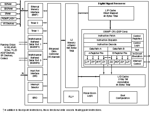
devices) compose the floating-point DSP family in the TMS320C6000™ DSP platform. The C6711, C6711B, C6711C, and C6711D devices are based on the high-performance, advanced very-long-instruction-word (VLIW) architecture developed by Texas Instruments (TI), making these DSPs an excellent choice for multichannel and multifunction applications.With performance of up to 1200 million floating-point operations per second (MFLOPS) at a clock rate of 200 MHz or up to 1500 MFLOPS at a clock rate of 250 MHz, the C6711D device also offers cost-effective solutions to high-performance DSP programming challenges. The C6711D DSP possesses the operational flexibility of high-speed controllers and the numerical capability of array processors. This processor has 32 general-purpose registers of 32-bit word length and eight highly independent functional units. The eight functional units provide four floating-/fixed-point ALUs, two fixed-point ALUs, and two floating-/fixed-point multipliers. The C6711D can produce two MACs per cycle for a total of 400 MMACS.The C6711D DSP also has application-specific hardware logic, on-chip memory, and additional on-chip peripherals.The C6711D device uses a two-level cache-based architecture and has a powerful and diverse set of peripherals. The Level 1 program cache (L1P) is a 32-Kbit direct mapped cache and the Level 1 data cache (L1D) is a 32-Kbit 2-way set-associative cache. The Level 2 memory/cache (L2) consists of a 512-Kbit memory space that is shared between program and data space. L2 memory can be configured as mapped memory, cache, or combinations of the two. The peripheral set includes two multichannel buffered serial ports (McBSPs), two general-purpose timers, a host-port interface (HPI), and a glueless external memory interface (EMIF) capable of interfacing to SDRAM, SBSRAM and asynchronous peripherals.The C6711D has a complete set of development tools which includes: a new C compiler, an assembly optimizer to simplify programming and scheduling, and a Windows™ debugger interface for visibility into source code execution.
TMS320C6711DZDP200 数据手册
| 数据手册 | 说明 | 数量 | 操作 |
|---|---|---|---|
 TMS320C6711DZDP200 TMS320C6711DZDP200
|
Floating-Point Digital Signal Processors 272-BGA |
38页,429K | 查看 |
TMS320C6711DZDP200 电路图
TMS320C6711DZDP200 电路图
TMS320C6711DZDP200 相关产品
- ADSP-2104BPZ-80
- ADSP-2105BPZ-80
- ADSP-21060CZ-160
- ADSP-21060KBZ-160
- ADSP-21060KSZ-133
- ADSP-21060LABZ-160
- ADSP-21060LCB-133
- ADSP-21060LCW-160
- ADSP-21060LKSZ-133
- ADSP-21061LASZ-176
- ADSP-21061LKSZ-176
- ADSP-21062KBZ-160
- ADSP-21062KSZ-160
- ADSP-21062LCSZ-160
- ADSP-21062LKBZ-160
- ADSP-21065LCCAZ240
- ADSP-21065LKCAZ264
- ADSP-21160NCB-100
- ADSP-21160NCBZ-100
- ADSP-21160NKBZ-100
- ADSP-21161NKCAZ100
- ADSP-21261SKSTZ150
- ADSP-21262SBBC-150
- ADSP-21262SBBCZ150
- ADSP-21266SKBCZ-2D
- ADSP-21266SKSTZ-1D
- ADSP-21266SKSTZ-2D
- ADSP-21362BSWZ-1AA
- ADSP-21363BBC-1AA
- ADSP-21363YSWZ-2AA