 搜索
搜索
 发布采购
发布采购
更新日期:2024-04-01 00:04:00

产品简介:多核数字信号处理器
查看详情TMS320C6474FCUNA 供应商
- 公司
- 型号
- 品牌
- 封装/批号
- 数量
- 地区
- 日期
- 说明
- 询价
-
TI
-
原厂原装
22+ -
3288
-
上海市
-
-
-
一级代理原装
TMS320C6474FCUNA 中文资料属性参数
- 现有数量:0现货查看交期
- 价格:60 : ¥2,135.18083托盘
- 系列:TMS320C647x
- 包装:托盘
- 产品状态:在售
- 类型:定点
- 接口:以太网 MAC,I2C,McBSP
- 时钟速率:1GHz
- 非易失性存储器:ROM(64kB)
- 片载 RAM:3.168MB
- 电压 - I/O:1.1V,1.8V
- 电压 - 内核:1.10V
- 工作温度:-40°C ~ 100°C(TC)
- 安装类型:表面贴装型
- 封装/外壳:561-BFBGA,FCCSPBGA
- 供应商器件封装:561-FC/CSP(23x23)
产品特性
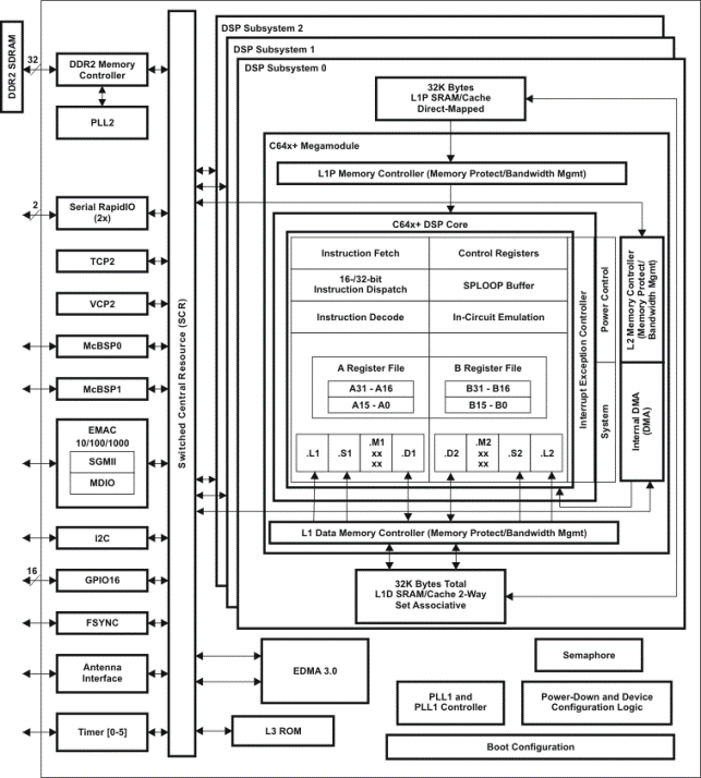
- Key Features High-Performance Multicore DSP (C6474) Instruction Cycle Time: 0.83 ns (1.2-GHz Device); 1 ns (1-GHz Device); 1.18 ns (850-MHz Device) Clock Rate: 1 GHz to 1.2 GHz (1.2-GHz Device); 1 GHz (1-GHz Device); 850 MHz (850-MHz Device) Commercial Temperature and Extended Tmperature 3 TMS320C64x+™ DSP Cores; Six RSAs for CDMA Processing (2 per core) Enhanced VCP2/TCP2 Frame Synchronization Interface 16-/32-Bit DDR2-667 Memory Controller EDMA3 Controller Antenna Interface Two 1x Serial RapidIO® Links, v1.2 Compliant One 1.8-V Inter-Integrated Circuit (I2C) Bus Two 1.8-V McBSPs 1000 Mbps Ethernet MAC (EMAC) Six 64-Bit General-Purpose Timers 16 General-Purpose I/O (GPIO) Pins Internal Semaphore Module non-UMTS Systems System PLL and PLL Controller/DDR PLL and PLL Controller, Dedicated to DDR2 Memory Controller
- High-Performance Multicore DSP (C6474)
- Instruction Cycle Time: 0.83 ns (1.2-GHz Device); 1 ns (1-GHz Device); 1.18 ns (850-MHz Device)
- Clock Rate: 1 GHz to 1.2 GHz (1.2-GHz Device); 1 GHz (1-GHz Device); 850 MHz (850-MHz Device)
- Commercial Temperature and Extended Tmperature
- 3 TMS320C64x+™ DSP Cores; Six RSAs for CDMA Processing (2 per core)
- Enhanced VCP2/TCP2
- Frame Synchronization Interface
- 16-/32-Bit DDR2-667 Memory Controller
- EDMA3 Controller
- Antenna Interface
- Two 1x Serial RapidIO® Links, v1.2 Compliant
- One 1.8-V Inter-Integrated Circuit (I2C) Bus
- Two 1.8-V McBSPs
- 1000 Mbps Ethernet MAC (EMAC)
- Six 64-Bit General-Purpose Timers
- 16 General-Purpose I/O (GPIO) Pins
- Internal Semaphore Module non-UMTS Systems
- System PLL and PLL Controller/DDR PLL and PLL Controller, Dedicated to DDR2 Memory Controller
- High-Performance Multicore DSP (C6474) Instruction Cycle Time: 1.2-GHz Device: 1.0-ns to 0.83-ns 1-GHz Device: 1-ns 850-MHz Device: 1.18 ns Clock Rate: 1.2-GHz Device: 1-GHz to 1.2-GHz 1-GHz Device: 1-GHz 850-MHz Device: 850 MHz Eight 32-Bit Instructions/Cycle Commercial Temperature: 1.2-GHz Device: 0°C to 95°C 1-GHz Device: 0°C to 100°C 850-MHZ and 1-GHz Device: 0°C to 100°C Extended Temperature: 1.2-GHz Device: -40°C to 95°C(1) 1-GHz Device: -40°C to 100°C
- Instruction Cycle Time: 1.2-GHz Device: 1.0-ns to 0.83-ns 1-GHz Device: 1-ns 850-MHz Device: 1.18 ns
- 1.2-GHz Device: 1.0-ns to 0.83-ns
- 1-GHz Device: 1-ns
- 850-MHz Device: 1.18 ns
- Clock Rate: 1.2-GHz Device: 1-GHz to 1.2-GHz 1-GHz Device: 1-GHz 850-MHz Device: 850 MHz
- 1.2-GHz Device: 1-GHz to 1.2-GHz
- 1-GHz Device: 1-GHz
- 850-MHz Device: 850 MHz
- Eight 32-Bit Instructions/Cycle
- Commercial Temperature: 1.2-GHz Device: 0°C to 95°C 1-GHz Device: 0°C to 100°C 850-MHZ and 1-GHz Device: 0°C to 100°C
- 1.2-GHz Device: 0°C to 95°C
- 1-GHz Device: 0°C to 100°C
- 850-MHZ and 1-GHz Device: 0°C to 100°C
- Extended Temperature: 1.2-GHz Device: -40°C to 95°C(1) 1-GHz Device: -40°C to 100°C
- 1.2-GHz Device: -40°C to 95°C(1)
- 1-GHz Device: -40°C to 100°C
- Dedicated SPLOOP Instructions
- Compact Instructions (16-Bit)
- Exception Handling
- 256 K-Bit (32 K-Byte) L1P Program Cache [Direct Mapped]
- 256 K-Bit (32 K-Byte) L1D Data Cache [2-Way Set-Associative]
- 512 K-Bit (64 K-Byte) L3 ROM
- Supports Over 694 7.95-Kbps AMR
- Supports up to Eight 2-Mbps 3 GPP (6 Iterations)
- Time Alignment Between Internal Subsystems, External Devices/System
- OBSAI RP1 Compliant for Frame Burst Data
- Alternate Interfaces for non-RP1 and non-UMTS Systems
- 6 Configurable Links (Full Duplex)
- Supports OBSAI RP3 Protocol, v1.0: 768-Mbps, 1.536-, 3.072-Gbps Link Rates
- Supports CPRI Protocol V2.0:614.4-Mbps, 1.2288-, 2.4576-Gbps Link Rates
- Clock Input Independent or Shared with CPU (Selectable at Boot-Time)
- 1.25-, 2.5-, 3.125-Gbps Link Rates
- Message Passing and DirectIO Support
- Error Management Extensions and Congestion Control
- IEEE 802.3 Compliant
- Supports SGMII, v1.8 Compliant
- 8 Independent Transmit (TX) and 8 Independent Receive (RX) Channels
- Configurable up to Twelve 32-Bit Timers
- Configurable in a Watchdog Timer mode
- Software Method to Control Access to Shared Resources
- 32 General Purpose Semaphore Resources
产品概述
The TMS320C64x+ DSPs (including the TMS320C6474 device) are the highest-performance multicore DSP generation in the TMS320C6000™ DSP platform.The C6474 device is based on the third-generation high-performance, advanced VelociTI™ very-long-instruction-word (VLIW) architecture developed by Texas Instruments (TI).The C64x+™ devices are upward code-compatible from previous devices that are part of the C6000™ DSP platform.
TMS320C6474FCUNA 电路图
TMS320C6474FCUNA 电路图
TMS320C6474FCUNA 相关产品
- 14305R-2000
- 3530ECUSAGRM
- 5CEBA2F23C8N
- 5CEBA2U15C6N
- 5CEBA2U15C8N
- 5CEBA2U15I7N
- 5CEBA2U19C8N
- 5CEBA4U15C7N
- 5CEBA4U15C8N
- 5CEBA4U19C7N
- 5CEBA5U19C8N
- 5CEBA7F31C8N
- 5CEBA9F23C7N
- 5CEBA9F23C8N
- 5CEBA9F31C7N
- 5CEFA2F23C6N
- 5CEFA4F23C7N
- 5CEFA4F23I7N
- 5CEFA4U19C6N
- 5CEFA4U19C8N
- 5CEFA5F23C6N
- 5CEFA5F23I7N
- 5CEFA5U19C7N
- 5CEFA7F23C6N
- 5CEFA7F23C7N
- 5CEFA7F27I7N
- 5CEFA7F31C7N
- 5CEFA7F31I7N
- 5CEFA7U19A7N
- 5CEFA9F23C7N