 搜索
搜索
 发布采购
发布采购
- 封装:20-SOIC(0.295",7.50mm 宽)
- RoHS:无铅 / 符合限制有害物质指令(RoHS)规范要求
- 包装方式:管件
- 参考价格:$10.33-$8.4664
更新日期:2024-04-01 00:04:00

产品简介:单通道 12 位并行电压输出 DAC,具有可编程内部基准、稳定时间和功耗
查看详情- 封装:20-SOIC(0.295",7.50mm 宽)
- RoHS:无铅 / 符合限制有害物质指令(RoHS)规范要求
- 包装方式:管件
- 参考价格:$10.33-$8.4664
TLV5639CDW 供应商
- 公司
- 型号
- 品牌
- 封装/批号
- 数量
- 地区
- 日期
- 说明
- 询价
-
TI
-
原厂原装
22+ -
3288
-
上海市
-
-
-
一级代理原装
-
TI(德州仪器)
-
SOIC-20
2022+ -
12000
-
上海市
-
-
-
原装可开发票
TLV5639CDW 中文资料属性参数
- 产品培训模块:Data Converter Basics
- 标准包装:25
- 类别:集成电路 (IC)
- 家庭:数据采集 - 数模转换器
- 系列:-
- 设置时间:3.5µs
- 位数:12
- 数据接口:并联
- 转换器数目:1
- 电压电源:单电源
- 功率耗散(最大):2.7mW
- 工作温度:0°C ~ 70°C
- 安装类型:表面贴装
- 封装/外壳:20-SOIC(0.295",7.50mm 宽)
- 供应商设备封装:20-SOIC
- 包装:管件
- 输出数目和类型:1 电压,单极
- 采样率(每秒):286k
- 配用:296-10736-ND - EVAL MOD FOR TLV5619-TLV5639
- 其它名称:296-2318-5
产品特性
- 12-Bit Voltage Output DAC
- Programmable Internal Reference
- Programmable Settling Time vs Power Consumption 1 µs in Fast Mode 3.5 µs in Slow Mode
- 1 µs in Fast Mode
- 3.5 µs in Slow Mode
- Compatible With TMS320
- Differential Nonlinearity...<0.5 LSB Typ
- Voltage Output Range ... 2x the Reference Voltage
- Monotonic Over Temperature
- APPLICATIONS Digital Servo Control Loops Digital Offset and Gain Adjustment Industrial Process Control Machine and Motion Control Devices Mass Storage Devices
- Digital Servo Control Loops
- Digital Offset and Gain Adjustment
- Industrial Process Control
- Machine and Motion Control Devices
- Mass Storage Devices
产品概述
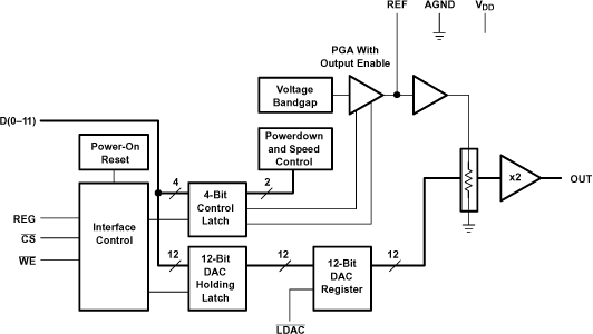
The TLV5639 is a 12-bit voltage output digital-to-analog converter (DAC) with a microprocessor compatible parallel interface. It is programmed with a 16-bit data word containing 4 control and 12 data bits. Developed for a wide range of supply voltages, the TLV5639 can be operated from 2.7 V to 5.5 V.The resistor string output voltage is buffered by a x2 gain rail-to-rail output buffer. The buffer features a ClassAB output stage to improve stability and reduce settling time. The programmable settling time of the DAC allows the designer to optimize speed versus power dissipation. Because of its ability to source up to 1 mA, the internal reference can also be used as a system reference. With its on-chip programmable precision voltage reference, the TLV5639 simplifies overall system design. The settling time and the reference voltage can be chosen by the control bits within the 16-bit data word.Implemented with a CMOS process, the device is designed for single supply operation from 2.7 V to 5.5 V. It is available in 20-pin SOIC and TSSOP packages in standard commercial and industrial temperature ranges.
TLV5639CDW 数据手册
| 数据手册 | 说明 | 数量 | 操作 |
|---|---|---|---|
 TLV5639CDW TLV5639CDW
|
2.7 V TO 5.5 V LOW POWER 12-BIT DIGITAL-TO-ANALOG CONVERTERS WITH INTERNAL REFERENCE AND POWER DOWN |
17 Pages页,243K | 查看 |
TLV5639CDW 电路图
TLV5639CDW 电路图
TLV5639CDW 相关产品
- AD1833AASTZ
- AD1851RZ-J
- AD1851RZ-REEL7
- AD1852JRSZRL
- AD1856RZ
- AD1859JRZ-RL
- AD1866RZ-REEL
- AD1933WBSTZ
- AD1934WBSTZ
- AD1953YSTZ
- AD1954YSTZ
- AD1954YSTZRL
- AD1955ARSZ
- AD1955ARSZRL
- AD420AR-32-REEL
- AD420ARZ-32
- AD420ARZ-32-REEL
- AD421BR
- AD421BRZ
- AD421BRZRL
- AD421BRZRL7
- AD5024BRUZ
- AD5024BRUZ-REEL7
- AD5025BRUZ
- AD5040BRJZ-REEL7
- AD5044BRUZ
- AD5060ARJZ-2REEL7
- AD5060BRJZ-1500RL7
- AD5060BRJZ-1REEL7
- AD5060BRJZ-2500RL7