 搜索
搜索
 发布采购
发布采购
- 封装:20-SOIC(0.295",7.50mm 宽)
- RoHS:无铅 / 符合限制有害物质指令(RoHS)规范要求
- 包装方式:管件
- 参考价格:$10.251-$9.34652
更新日期:2024-04-01 00:04:00

产品简介:具有可编程内部基准电压、稳定时间及功耗、8 位微控制器兼容接口的 12 位并行电压输出 DAC
查看详情- 封装:20-SOIC(0.295",7.50mm 宽)
- RoHS:无铅 / 符合限制有害物质指令(RoHS)规范要求
- 包装方式:管件
- 参考价格:$10.251-$9.34652
TLV5633IDW 供应商
- 公司
- 型号
- 品牌
- 封装/批号
- 数量
- 地区
- 日期
- 说明
- 询价
-
TI
-
原厂原装
22+ -
3288
-
上海市
-
-
-
一级代理原装
-
TI/德州仪器
-
SOIC20
21+ -
10000
-
杭州
-
-
-
原装正品,BOM一站式服务
-
TI
-
-
2019+ -
5800
-
上海市
-
-
-
全新原装现货
-
TI(德州仪器)
-
SOIC-20
2022+ -
12000
-
上海市
-
-
-
原装可开发票
-
TI
-
SOIC20
22+ -
300000
-
常州
-
-
-
原装正品
-
TI
-
SOP20
23+ -
5800
-
上海市
-
-
-
进口原装现货,杜绝假货。
-
-
23+ -
46000
-
合肥
-
-
-
科大讯飞战略投资企业,提供一站式配套服务
TLV5633IDW 中文资料属性参数
- 产品培训模块:Data Converter Basics
- 标准包装:25
- 类别:集成电路 (IC)
- 家庭:数据采集 - 数模转换器
- 系列:-
- 设置时间:3.5µs
- 位数:12
- 数据接口:并联
- 转换器数目:1
- 电压电源:模拟和数字
- 功率耗散(最大):2.7mW
- 工作温度:-40°C ~ 85°C
- 安装类型:表面贴装
- 封装/外壳:20-SOIC(0.295",7.50mm 宽)
- 供应商设备封装:20-SOIC
- 包装:管件
- 输出数目和类型:1 电压,单极
- 采样率(每秒):286k
- 其它名称:296-3071-5
产品特性
- 12-Bit Voltage Output DAC
- Programmable Internal Reference
- Programmable Settling Time vs Power Consumption 1 µs in Fast Mode3.5 µs in Slow Mode
- 1 µs in Fast Mode
- 3.5 µs in Slow Mode
- 8-Bit µController Compatible Interface
- Differential Nonlinearity. . .<0.5 LSB Typ
- Voltage Output Range. . .2x the Reference Voltage
- Monotonic Over Temperature
- APPLICATIONSDigital Servo Control LoopsDigital Offset and Gain AdjustmentIndustrial Process ControlMachine and Motion Control DevicesMass Storage Devices
- Digital Servo Control Loops
- Digital Offset and Gain Adjustment
- Industrial Process Control
- Machine and Motion Control Devices
- Mass Storage Devices
产品概述
The TLV5633 is a 12-bit voltage output digital- to-analog converter (DAC) with an 8-bit microcontroller compatible parallel interface. The 8 LSBs, the 4 MSBs, and 5 control bits are written using three different addresses. Developed for a wide range of supply voltages, the TLV5633 can be operated from 2.7 V to 5.5 V.The resistor string output voltage is buffered by a x2 gain rail-to-rail output buffer. The buffer features a Class A (slow mode: AB) output stage to improve stability and reduce settling time. The programmable settling time of the DAC allows the designer to optimize speed versus power dissipation. With its on-chip programmable precision voltage reference, the TLV5633 simplifies overall system design. Because of its ability to source up to 1 mA, the internal reference can also be used as a system reference. The settling time and the reference voltage can be chosen by a control register.Implemented with a CMOS process, the device is designed for single supply operation from 2.7 V to 5.5 V. It is available in 20-pin SOIC and TSSOP packages in standard commercial and industrial temperature ranges.
TLV5633IDW 数据手册
| 数据手册 | 说明 | 数量 | 操作 |
|---|---|---|---|
 TLV5633IDW TLV5633IDW
|
2.7 V TO 5.5 V LOW POWER 12-BIT DIGITAL-TO-ANALOG CONVERTERS WITH INTERNAL REFERENCE AND POWER DOWN |
22 Pages页,302K | 查看 |
|
TLV5633IDW
|
12 Bit Digital to Analog Converter 1 20-SOIC |
26页,588K | 查看 |
TLV5633IDW 电路图
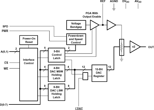
TLV5633IDW 电路图
TLV5633IDW 相关产品
- AD1833AASTZ
- AD1851RZ-J
- AD1851RZ-REEL7
- AD1852JRSZRL
- AD1856RZ
- AD1859JRZ-RL
- AD1866RZ-REEL
- AD1933WBSTZ
- AD1934WBSTZ
- AD1953YSTZ
- AD1954YSTZ
- AD1954YSTZRL
- AD1955ARSZ
- AD1955ARSZRL
- AD420AR-32-REEL
- AD420ARZ-32
- AD420ARZ-32-REEL
- AD421BR
- AD421BRZ
- AD421BRZRL
- AD421BRZRL7
- AD5024BRUZ
- AD5024BRUZ-REEL7
- AD5025BRUZ
- AD5040BRJZ-REEL7
- AD5044BRUZ
- AD5060ARJZ-2REEL7
- AD5060BRJZ-1500RL7
- AD5060BRJZ-1REEL7
- AD5060BRJZ-2500RL7