 搜索
搜索
 发布采购
发布采购
- 封装:20-SOIC(0.295",7.50mm 宽)
- RoHS:无铅 / 符合限制有害物质指令(RoHS)规范要求
- 包装方式:管件
- 参考价格:$12-$9.84
更新日期:2024-04-01 00:04:00

产品简介:具有串行输入、可编程稳定时间/功耗、低功耗、关断、内部基准的 8 位、8 通道、1/3us DAC
查看详情- 封装:20-SOIC(0.295",7.50mm 宽)
- RoHS:无铅 / 符合限制有害物质指令(RoHS)规范要求
- 包装方式:管件
- 参考价格:$12-$9.84
TLV5632IDW 供应商
- 公司
- 型号
- 品牌
- 封装/批号
- 数量
- 地区
- 日期
- 说明
- 询价
-
TI
-
原厂原装
22+ -
3288
-
上海市
-
-
-
一级代理原装
-
TI
-
-
2019+ -
5800
-
上海市
-
-
-
全新原装现货
-
TI(德州仪器)
-
SOIC-20
2022+ -
12000
-
上海市
-
-
-
原装可开发票
TLV5632IDW 中文资料属性参数
- 产品培训模块:Data Converter Basics
- 标准包装:25
- 类别:集成电路 (IC)
- 家庭:数据采集 - 数模转换器
- 系列:-
- 设置时间:3µs
- 位数:8
- 数据接口:串行
- 转换器数目:8
- 电压电源:模拟和数字
- 功率耗散(最大):48mW
- 工作温度:-40°C ~ 85°C
- 安装类型:表面贴装
- 封装/外壳:20-SOIC(0.295",7.50mm 宽)
- 供应商设备封装:20-SOIC
- 包装:管件
- 输出数目和类型:8 电压,单极
- 采样率(每秒):283k
- 其它名称:296-3069-5
产品特性
- Eight Voltage Output DACs in One Package TLV5630 . . .12-Bit TLV5631 . . .10-Bit TLV5632 . . .8-Bit 1 µs in Fast Mode3 µs in Slow Mode
- TLV5630 . . .12-Bit
- TLV5631 . . .10-Bit
- TLV5632 . . .8-Bit
- 1 µs in Fast Mode
- 3 µs in Slow Mode
- Programmable Settling Time vs Power Consumption 1 µs in Fast Mode3 µs in Slow Mode18 mW in Slow Mode at 3 V48 mW in Fast Mode at 3 V
- 1 µs in Fast Mode
- 3 µs in Slow Mode
- 18 mW in Slow Mode at 3 V
- 48 mW in Fast Mode at 3 V
- Compatible With TMS320 and SPI Serial Ports
- Monotonic Over Temperature
- Low Power Consumption: 18 mW in Slow Mode at 3 V48 mW in Fast Mode at 3 V
- 18 mW in Slow Mode at 3 V
- 48 mW in Fast Mode at 3 V
- Power-Down Mode
- Internal Reference
- Data Output for Daisy-Chaining
- APPLICATIONSDigital Servo Control LoopsDigital Offset and Gain AdjustmentIndustrial Process ControlMachine and Motion Control DevicesMass Storage Devices
- Digital Servo Control Loops
- Digital Offset and Gain Adjustment
- Industrial Process Control
- Machine and Motion Control Devices
- Mass Storage Devices
产品概述
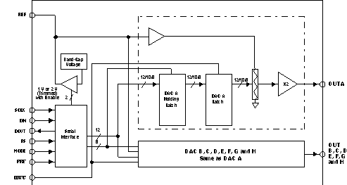
The TLV5630, TLV5631, and TLV5632 are pin-compatible,
eight-channel, 12-/10-/8-bit voltage output DACs each with a flexible serial
interface. The serial interface allows glueless interface to TMS320 and SPI,
QSPI, and Microwire serial ports. It is programmed with a 16-bit serial string
containing 4 control and 12 data bits.Additional features are a power-down mode, an
LDAC input for simultaneous update of all
eight DAC outputs, and a data output which can be used to cascade multiple
devices, and an internal programmable band-gap reference.The resistor string output voltage is buffered by a
rail-to-rail output amplifier with a programmable settling time to allow the
designer to optimize speed vs power dissipation. The buffered, high-impedance
reference input can be connected to the supply voltage.Implemented with a CMOS process, the DACs are designed for
single-supply operation from 2.7 V to 5.5 V, and can operate on two separate analog and digital power supplies. The devices are available in
20-pin SOIC and TSSOP packages.
TLV5632IDW 数据手册
| 数据手册 | 说明 | 数量 | 操作 |
|---|---|---|---|
 TLV5632IDW TLV5632IDW
|
8-CHANNEL, 12-/10-/8-BIT, 2.7-V TO 5.5-V LOW POWER DIGITAL-TO-ANALOG CONVERTERS WITH POWER DOWN AND INTERNAL REFERENCE |
15 Pages页,273K | 查看 |
|
TLV5632IDW
|
8 Bit Digital to Analog Converter 8 20-SOIC |
24页,1.13M | 查看 |
TLV5632IDW 电路图
TLV5632IDW 电路图
TLV5632IDW 相关产品
- AD1833AASTZ
- AD1851RZ-J
- AD1851RZ-REEL7
- AD1852JRSZRL
- AD1856RZ
- AD1859JRZ-RL
- AD1866RZ-REEL
- AD1933WBSTZ
- AD1934WBSTZ
- AD1953YSTZ
- AD1954YSTZ
- AD1954YSTZRL
- AD1955ARSZ
- AD1955ARSZRL
- AD420AR-32-REEL
- AD420ARZ-32
- AD420ARZ-32-REEL
- AD421BR
- AD421BRZ
- AD421BRZRL
- AD421BRZRL7
- AD5024BRUZ
- AD5024BRUZ-REEL7
- AD5025BRUZ
- AD5040BRJZ-REEL7
- AD5044BRUZ
- AD5060ARJZ-2REEL7
- AD5060BRJZ-1500RL7
- AD5060BRJZ-1REEL7
- AD5060BRJZ-2500RL7