 搜索
搜索
 发布采购
发布采购
- 封装:8-TSSOP,8-MSOP(0.118",3.00mm 宽)
- RoHS:无铅 / 符合限制有害物质指令(RoHS)规范要求
- 包装方式:管件
- 参考价格:$6.437
更新日期:2024-04-01 00:04:00
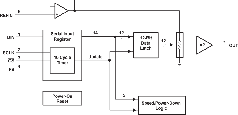
产品简介:可编程建立时间与功耗关系得到优化的 12 位、单通道、低功耗电压输出 DAC
查看详情- 封装:8-TSSOP,8-MSOP(0.118",3.00mm 宽)
- RoHS:无铅 / 符合限制有害物质指令(RoHS)规范要求
- 包装方式:管件
- 参考价格:$6.437
TLV5616CDGK 供应商
- 公司
- 型号
- 品牌
- 封装/批号
- 数量
- 地区
- 日期
- 说明
- 询价
-
TI
-
原厂原装
22+ -
3288
-
上海市
-
-
-
一级代理原装
TLV5616CDGK 中文资料属性参数
- 产品培训模块:Data Converter Basics
- 标准包装:80
- 类别:集成电路 (IC)
- 家庭:数据采集 - 数模转换器
- 系列:-
- 设置时间:9µs
- 位数:12
- 数据接口:串行
- 转换器数目:1
- 电压电源:单电源
- 功率耗散(最大):2.1mW
- 工作温度:0°C ~ 70°C
- 安装类型:表面贴装
- 封装/外壳:8-TSSOP,8-MSOP(0.118",3.00mm 宽)
- 供应商设备封装:8-MSOP
- 包装:管件
- 输出数目和类型:1 电压,单极
- 采样率(每秒):102k
产品特性
- 12-Bit Voltage Output DAC
- Programmable Settling Time vs Power Consumption 3 µs in Fast Mode 9 µs in Slow Mode
- 3 µs in Fast Mode
- 9 µs in Slow Mode
- Ultra Low Power Consumption:
- 900 µW Typ in Slow Mode at 3 V
- 2.1 mW Typ in Fast Mode at 3 V
- Differential Nonlinearity . . . <0.5 LSB Typ
- Compatible With TMS320 and SPI Serial Ports
- Power-Down Mode (10 nA)
- Buffered High-Impedance Reference Input
- Voltage Output Range . . . 2 Times the Reference Input Voltage
- Monotonic Over Temperature
- Available in MSOP Package
产品概述
The TLV5616 is a 12-bit voltage output digital-to-analog converter (DAC) with a flexible 4-wire serial interface. The 4-wire serial interface allows glueless interface to TMS320, SPI, QSPI, and Microwire serial ports. The TLV5616 is programmed with a 16-bit serial string containing 4 control and 12 data bits. Developed for a wide
range of supply voltages, the TLV5616 can operate from 2.7 V to 5.5 V.The resistor string output voltage is buffered by a x2 gain rail-to-rail output buffer. The buffer features a Class AB output stage to improve stability and reduce settling time. The settling time of the DAC is programmable to allow the designer to optimize speed versus power dissipation. The settling time is chosen by the control bits within the 16-bit serial input string. A high-impedance buffer is integrated on the REFIN terminal to reduce the need for a low source impedance drive to the terminal.Implemented with a CMOS process, the TLV5616 is designed for single supply operation from 2.7 V to 5.5 V. The device is available in an 8-terminal SOIC package. The TLV5616C is characterized for operation from 0°C to 70°C. The TLV5616I is characterized for operation from -40°C to 85°C.
TLV5616CDGK 数据手册
| 数据手册 | 说明 | 数量 | 操作 |
|---|---|---|---|
 TLV5616CDGK TLV5616CDGK
|
2.7 V TO 5.5 V LOW POWER 12-BIT DIGITAL-TO-ANALOG CONVERTERS WITH POWER DOWN |
23 Pages页,311K | 查看 |
|
TLV5616CDGK
|
12 Bit Digital to Analog Converter 1 8-VSSOP |
29页,1.07M | 查看 |
TLV5616CDGK 电路图
TLV5616CDGK 电路图
TLV5616CDGK 相关产品
- AD1833AASTZ
- AD1851RZ-J
- AD1851RZ-REEL7
- AD1852JRSZRL
- AD1856RZ
- AD1859JRZ-RL
- AD1866RZ-REEL
- AD1933WBSTZ
- AD1934WBSTZ
- AD1953YSTZ
- AD1954YSTZ
- AD1954YSTZRL
- AD1955ARSZ
- AD1955ARSZRL
- AD420AR-32-REEL
- AD420ARZ-32
- AD420ARZ-32-REEL
- AD421BR
- AD421BRZ
- AD421BRZRL
- AD421BRZRL7
- AD5024BRUZ
- AD5024BRUZ-REEL7
- AD5025BRUZ
- AD5040BRJZ-REEL7
- AD5044BRUZ
- AD5060ARJZ-2REEL7
- AD5060BRJZ-1500RL7
- AD5060BRJZ-1REEL7
- AD5060BRJZ-2500RL7