 搜索
搜索
 发布采购
发布采购
- 封装:16-TSSOP(0.173",4.40mm 宽)
- RoHS:无铅 / 符合限制有害物质指令(RoHS)规范要求
- 包装方式:管件
- 参考价格:$12.888-$21.48
更新日期:2024-04-01 00:04:00

产品简介:具有串行输入、可编程稳定时间、低功耗和硬件或软件断电功能的 12 位 3us 四通道 DAC
查看详情- 封装:16-TSSOP(0.173",4.40mm 宽)
- RoHS:无铅 / 符合限制有害物质指令(RoHS)规范要求
- 包装方式:管件
- 参考价格:$12.888-$21.48
TLV5614CPW 供应商
- 公司
- 型号
- 品牌
- 封装/批号
- 数量
- 地区
- 日期
- 说明
- 询价
-
TI
-
原厂原装
22+ -
3288
-
上海市
-
-
-
一级代理原装
-
TI/德州仪器
-
TSSOP16
2024 -
89832
-
上海市
-
-
-
上海原装现货库存,欢迎咨询合作
-
TI(德州仪器)
-
TSSOP-16
2022+ -
12000
-
上海市
-
-
-
原装可开发票
-
TI
-
TSSOP16
23+ -
5800
-
上海市
-
-
-
进口原装现货,杜绝假货。
-
TI/德州仪器
-
21+
TSSOP16 -
10000
-
杭州
-
-
-
只做原装现货,大量现货热卖
TLV5614CPW 中文资料属性参数
- 产品培训模块:Data Converter Basics
- 标准包装:90
- 类别:集成电路 (IC)
- 家庭:数据采集 - 数模转换器
- 系列:-
- 设置时间:9µs
- 位数:12
- 数据接口:串行
- 转换器数目:4
- 电压电源:模拟和数字
- 功率耗散(最大):8.0mW
- 工作温度:0°C ~ 70°C
- 安装类型:表面贴装
- 封装/外壳:16-TSSOP(0.173",4.40mm 宽)
- 供应商设备封装:16-TSSOP
- 包装:管件
- 输出数目和类型:4 电压,单极
- 采样率(每秒):102k
- 其它名称:296-3040-5
产品特性
- Four 12-Bit D/A Converters
- Programmable Settling Time of Either 3 µs or 9 µs Typ
- TMS320, (Q)SPI™, and Microwire™ Compatible Serial Interface
- Internal Power-On Reset
- Low Power Consumption: 8 mW, Slow Mode – 5-V Supply 3.6 mW, Slow Mode – 3-V Supply
- Reference Input Buffer
- Voltage Output Range ...2× the Reference Input Voltage
- Monotonic Over Temperature
- Dual 2.7-V to 5.5-V Supply (Separate Digital and Analog Supplies)
- Hardware Power Down (10 nA)
- Software Power Down (10 nA)
- Simultaneous Update
- applications Battery Powered Test Instruments Digital Offset and Gain Adjustment Industrial Process Controls Machine and Motion Control Devices Communications Arbitrary Waveform Generation
- Battery Powered Test Instruments
- Digital Offset and Gain Adjustment
- Industrial Process Controls
- Machine and Motion Control Devices
- Communications
- Arbitrary Waveform Generation
产品概述
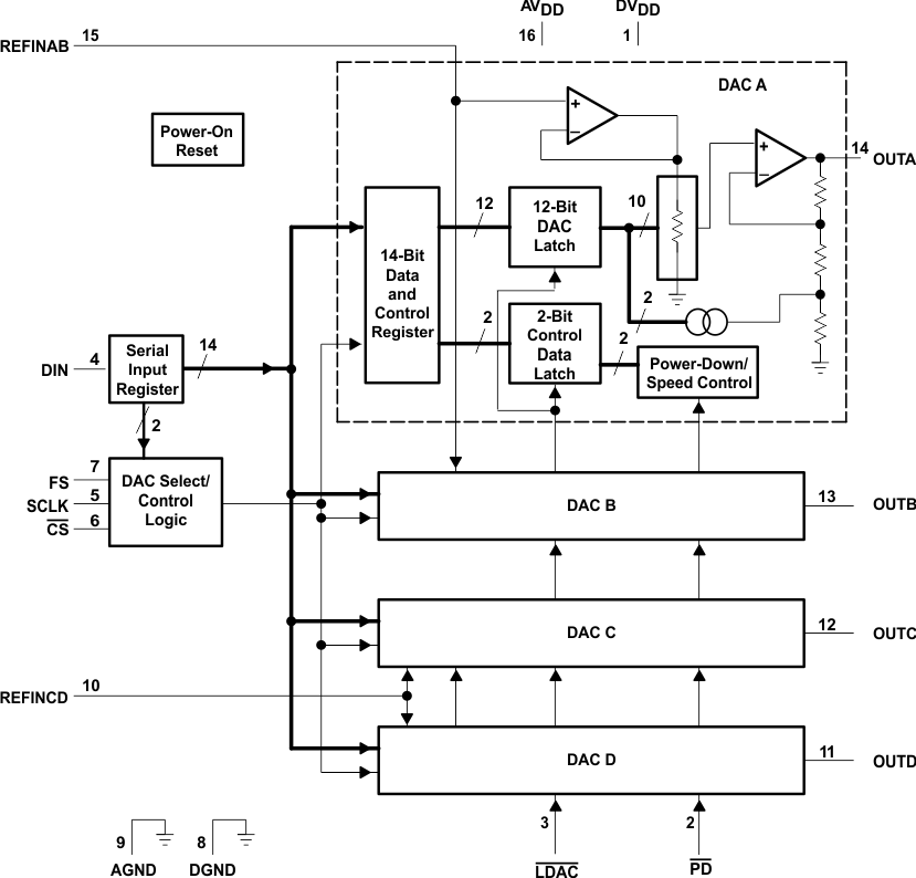
The TLV5614 is a quadruple 12-bit voltage output
digital-to-analog converter (DAC) with a flexible
4-wire serial interface. The 4-wire serial interface
allows glueless interface to TMS320, SPI, QSPI,
and Microwire serial ports. The TLV5614 is
programmed with a 16-bit serial word comprised
of a DAC address, individual DAC control bits, and
a 12-bit DAC value. The device has provision for
two supplies: one digital supply for the serial
interface (via pins DVDD and DGND), and one for
the DACs, reference buffers, and output buffers (via pins AVDD and AGND). Each supply is independent of the
other, and can be any value between 2.7 V and 5.5 V. The dual supplies allow a typical application where the
DAC will be controlled via a microprocessor operating on a 3 V supply (also used on pins DVDD and DGND),
with the DACs operating on a 5 V supply. Of course, the digital and analog supplies can be tied together.The resistor string output voltage is buffered by a x2 gain rail-to-rail output buffer. The buffer features a Class AB output stage to improve stability and reduce settling time. A rail-to-rail output stage and a power-down mode makes it ideal for single voltage, battery based applications. The settling time of the DAC is programmable to allow the designer to optimize speed versus power dissipation. The settling time is chosen by the control bits within the 16-bit serial input string. A high-impedance buffer is integrated on the REFINAB and REFINCD terminals to reduce the need for a low source impedance drive to the terminal. REFINAB and REFINCD allow DACs A and B to have a different reference voltage then DACs C and D.The TLV5614 is implemented with a CMOS process and is available in a 16-terminal SOIC package. The TLV5614C is characterized for operation from 0°C to 70°C. The TLV5614I is characterized for operation from –40°C to 85°C.
TLV5614CPW 电路图
TLV5614CPW 电路图
TLV5614CPW 相关产品
- AD1833AASTZ
- AD1851RZ-J
- AD1851RZ-REEL7
- AD1852JRSZRL
- AD1856RZ
- AD1859JRZ-RL
- AD1866RZ-REEL
- AD1933WBSTZ
- AD1934WBSTZ
- AD1953YSTZ
- AD1954YSTZ
- AD1954YSTZRL
- AD1955ARSZ
- AD1955ARSZRL
- AD420AR-32-REEL
- AD420ARZ-32
- AD420ARZ-32-REEL
- AD421BR
- AD421BRZ
- AD421BRZRL
- AD421BRZRL7
- AD5024BRUZ
- AD5024BRUZ-REEL7
- AD5025BRUZ
- AD5040BRJZ-REEL7
- AD5044BRUZ
- AD5060ARJZ-2REEL7
- AD5060BRJZ-1500RL7
- AD5060BRJZ-1REEL7
- AD5060BRJZ-2500RL7