 搜索
搜索
 发布采购
发布采购
- 封装:10-XFQFN
- RoHS:无铅 / 符合限制有害物质指令(RoHS)规范要求
- 包装方式:Digi-Reel®
- 参考价格:$0.496-$1.16
更新日期:2024-04-01 00:04:00

产品简介:双路、5.5V、2.2MHz 运算放大器
查看详情- 封装:10-XFQFN
- RoHS:无铅 / 符合限制有害物质指令(RoHS)规范要求
- 包装方式:Digi-Reel®
- 参考价格:$0.496-$1.16
TLV342IRUGR 供应商
- 公司
- 型号
- 品牌
- 封装/批号
- 数量
- 地区
- 日期
- 说明
- 询价
-
TI
-
原厂原装
22+ -
3288
-
上海市
-
-
-
一级代理原装
TLV342IRUGR 中文资料属性参数
- 标准包装:1
- 类别:集成电路 (IC)
- 家庭:Linear - Amplifiers - Instrumentation, OP Amps, Buffer Amps
- 系列:-
- 放大器类型:通用
- 电路数:2
- 输出类型:满摆幅
- 转换速率:1 V/µs
- 增益带宽积:2.3MHz
- -3db带宽:-
- 电流 - 输入偏压:1pA
- 电压 - 输入偏移:300µV
- 电流 - 电源:75µA
- 电流 - 输出 / 通道:115mA
- 电压 - 电源,单路/双路(±):1.5 V ~ 5.5 V
- 工作温度:-40°C ~ 125°C
- 安装类型:表面贴装
- 封装/外壳:10-XFQFN
- 供应商设备封装:10-X2QFN-EP(2x1.5)
- 包装:®
- 其它名称:296-24766-6
产品特性
- 1.8-V and 5-V Performance
- Low Offset (A Grade) 1.25 mV Maximum (25°C) 1.7 mV Maximum (–40°C to 125°C)
- 1.25 mV Maximum (25°C)
- 1.7 mV Maximum (–40°C to 125°C)
- Rail-to-Rail Output Swing
- Wide Common-Mode Input Voltage Range: –0.2 V to (V+ – 0.5 V)
- Input Bias Current: 1 pA (Typical)
- Input Offset Voltage: 0.3 mV (Typical)
- Low Supply Current: 70 µA/Channel
- Low Shutdown Current: 10 pA (Typical) Per Channel
- Gain Bandwidth: 2.3 MHz (Typical)
- Slew Rate: 0.9 V/µs (Typical)
- Turnon Time From Shutdown: 5 µs (Typical)
- Input Referred Voltage Noise (at 10 kHz): 20 nV/√Hz
- ESD Protection Exceeds JESD 22 2000-V Human-Body Model (HBM) 750-V Charged-device model (CDM)
- 2000-V Human-Body Model (HBM)
- 750-V Charged-device model (CDM)
产品概述
The TLV34xx devices are single and dual CMOS operational amplifiers, respectively, with
low-voltage, low-power, and rail-to-rail output swing capabilities. The PMOS input stage offers an
ultra-low input bias current of 1 pA (typical) and an offset voltage of
0.3 mV (typical). For applications requiring excellent dc precision, the A grade (TLV34xA)
has a low offset voltage of 1.25 mV (maximum) at 25°C.These single-supply amplifiers are designed specifically for ultra-low-voltage (1.5 V to
5 V) operation, with a common-mode input voltage range that typically extends from –0.2 V to 0.5 V
from the positive supply rail.The TLV341 (single) and TLV342 (dual) in the RUG package also offer a shutdown (SHDN) pin
that can be used to disable the device. In shutdown mode, the supply current is reduced to 45 pA
(typical). Offered in both the SOT-23 and smaller SC70 packages, the TLV341 is suitable for the
most space-constrained applications. The dual TLV342 is offered in the standard SOIC, VSSOP, and
X2QFN packages.An extended industrial temperature range from –40°C to 125°C makes the TLV34xx suitable
in a wide variety of commercial and industrial applications.
TLV342IRUGR 电路图
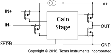
TLV342IRUGR 电路图
TLV342IRUGR 相关产品
- ACPL-7900-000E
- ACPL-7900-300E
- ACPL-790A-000E
- ACPL-790B-000E
- ACPL-790B-300E
- ACPL-C784-000E
- ACPL-C790-500E
- ACPL-C79A-500E
- ACPL-C79B-500E
- AD202JY
- AD202KN
- AD202KY
- AD210AN
- AD210BN
- AD521JDZ
- AD521KDZ
- AD521LDZ
- AD524AE
- AD524ARZ-16-REEL7
- AD524BE
- AD524CD
- AD526BDZ
- AD526CD
- AD526CDZ
- AD526JNZ
- AD526SD
- AD548JRZ-REEL
- AD548KNZ
- AD5748ACPZ-RL7
- AD5749ACPZ-RL7