 搜索
搜索
 发布采购
发布采购
- 封装:20-SOIC(0.295",7.50mm 宽)
- RoHS:无铅 / 符合限制有害物质指令(RoHS)规范要求
- 包装方式:带卷 (TR)
- 参考价格:$3.825
更新日期:2024-04-01 00:04:00

产品简介:具有断电功能的 12 位 200KSPS 11 通道低功耗串行 ADC
查看详情- 封装:20-SOIC(0.295",7.50mm 宽)
- RoHS:无铅 / 符合限制有害物质指令(RoHS)规范要求
- 包装方式:带卷 (TR)
- 参考价格:$3.825
TLV2553IDWR 供应商
- 公司
- 型号
- 品牌
- 封装/批号
- 数量
- 地区
- 日期
- 说明
- 询价
-
TI
-
原厂原装
22+ -
3288
-
上海市
-
-
-
一级代理原装
-
TI/德州仪器
-
SOIC20
21+ -
10000
-
杭州
-
-
-
原装正品,BOM一站式服务
-
TI/德州仪器
-
SOIC20
2022+ -
3000
-
上海市
-
-
-
原装可开发票
-
TI
-
TSSOP
23+ -
46000
-
合肥
-
-
-
科大讯飞战略投资企业,提供一站式配套服务
TLV2553IDWR 中文资料属性参数
- 产品培训模块:Data Converter Basics
- 标准包装:2,000
- 类别:集成电路 (IC)
- 家庭:数据采集 - 模数转换器
- 系列:-
- 位数:12
- 采样率(每秒):200k
- 数据接口:串行,SPI?
- 转换器数目:1
- 功率耗散(最大):-
- 电压电源:单电源
- 工作温度:-40°C ~ 85°C
- 安装类型:表面贴装
- 封装/外壳:20-SOIC(0.295",7.50mm 宽)
- 供应商设备封装:20-SOIC
- 包装:带卷 (TR)
- 输入数目和类型:11 个单端,单极
- 配用:296-18350-ND - KIT 5-6K INTERFACE BOARD
产品特性
- 12-Bit-Resolution A/D Converter
- Up to 200 KSPS (150 KSPS for 3 V) Throughput Over Operating Temperature Range With 12-Bit Output Mode
- 11 Analog Input Channels
- 3 Built-In Self-Test Modes
- Inherent Sample and Hold Function
- Linearity Error, ±1 LSB Maximum
- On-Chip Conversion Clock
- Unipolar or Bipolar Output Operation
- Programmable MSB or LSB First
- Programmable Power Down
- Programmable Output Data Length
- SPI Compatible Serial Interface With I/O Clock Frequencies up to 15 MHz (CPOL=0, CPHA=0)
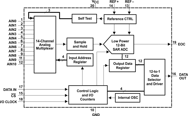
产品概述
The TLV2553 is a 12-bit, switched-capacitor, successive-approximation, analog-to-digital
converter. The ADC has three control inputs [chip select (CS), the
input-output clock, and the address/control input (DATAIN)], designed for communication with the
serial port of a host processor or peripheral through a serial 3-state output.In addition to the high-speed converter and versatile control capability, the device has
an on-chip 14-channel multiplexer that can select any one of 11 inputs or any one of three internal
self-test voltages using configuration register 1. The sample-and-hold function is automatic. At
the end of conversion, when programmed as EOC, the pin 19 output goes high to indicate that
conversion is complete. The converter incorporated in the device features differential, high-
impedance reference inputs that facilitate ratiometric conversion, scaling, and isolation of analog
circuitry from logic and supply noise. A switched-capacitor design allows low-error conversion over
the full operating temperature range.The TLV2553I is characterized for operation from
TA = –40°C to 85°C.
TLV2553IDWR 电路图
TLV2553IDWR 电路图
TLV2553IDWR 相关产品
- 6PADC3101TRGERQ1
- AD1674ARZ
- AD1674BRZ
- AD1674JNZ
- AD1674KRZ
- AD1974YSTZ
- AD5590BBCZ
- AD573KNZ
- AD574AJPZ
- AD574AKE
- AD574AKP
- AD574ALD
- AD574ALNZ
- AD6600ASTZ
- AD6600ASTZ-REEL
- AD6644ASTZ-40
- AD6645ASVZ-80
- AD6654CBC
- AD670JP
- AD670JPZ
- AD670JPZ-REEL7
- AD670KNZ
- AD673JNZ
- AD674BARZ
- AD674BJNZ
- AD674BKNZ
- AD676JDZ
- AD676JN
- AD676JNZ
- AD677JRZ-REEL