 搜索
搜索
 发布采购
发布采购
- 参考价格:¥84.32-¥87.01
更新日期:2024-04-01 00:04:00

产品简介:具有串行输出、自动断电(软件和硬件)、低功耗、8 x FIFO 和 8 通道的 2 位 200kSPS ADC(增强型产品)
查看详情- 参考价格:¥84.32-¥87.01
TLV2548MPWREP 供应商
- 公司
- 型号
- 品牌
- 封装/批号
- 数量
- 地区
- 日期
- 说明
- 询价
-
TI(德州仪器)
-
TSSOP-20
2022+ -
12000
-
上海市
-
-
-
原装可开发票
TLV2548MPWREP 中文资料属性参数
- 制造商:Texas Instruments
- 产品种类:ADC(模数转换器)
- 封装:Reel
- 工厂包装数量:2000
产品特性
- Maximum Throughput 200-KSPS
- Built-In Reference, Conversion Clock and 8x FIFO
- Differential/Integral Nonlinearity Error: ±1.2 LSB
- Signal-to-Noise and Distortion Ratio: 70 dB, fi = 12 kHz
- Spurious Free Dynamic Range: 75 dB, fi = 12 kHz
- SPI (CPOL = 0, CPHA = 0)/DSP-Compatible Serial Interfaces With SCLK up to 20 MHz
- Single Wide Range Supply 3.0 Vdc to 5.5 Vdc
- Analog Input Range 0 V to Supply Voltage With 500-kHz BW
- Hardware Controlled and Programmable Sampling Period
- Low Operating Current (1.0 mA at 3.3 V, 2.0 mA at 5.5 V With External Ref, 1.7-mA at 3.3V, 2.4-mA at 5.5-V With Internal Ref)
- Power Down: Software/Hardware Power-Down Mode (1 µA Max, Ext Ref), Autopower-Down Mode (1 µA, Ext Ref)
- Programmable Auto-Channel Sweep
- SUPPORTS DEFENSE, AEROSPACE, AND MEDICAL APPLICATIONS Controlled Baseline One Assembly/Test Site One Fabrication Site Available in Military (–55°C/125°C) Temperature Range(1) Extended Product Life Cycle Extended Product-Change Notification Product Traceability
- Controlled Baseline
- One Assembly/Test Site
- One Fabrication Site
- Available in Military (–55°C/125°C) Temperature Range(1)
- Extended Product Life Cycle
- Extended Product-Change Notification
- Product Traceability
产品概述
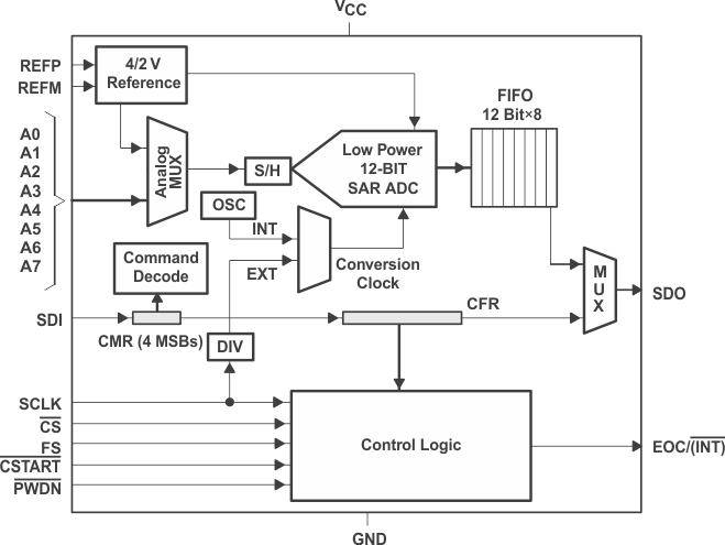
The TLV2548 is a high performance, 12-bit low-power, 3.86-µs, CMOS analog-to-digital converter (ADC) which operates from a single 3.0-V to 5.5-V power supply. This device has three digital inputs and a 3-state output [chip select (CS), serial input-output clock (SCLK), serial data input (SDI), and serial data output (SDO)] that provide a direct 4-wire interface to the serial port of most popular host microprocessors (SPI interface). When interfaced with a TI DSP, a frame sync (FS) signal is used to indicate the start of a serial data frame.In addition to a high-speed A/D converter and versatile control capability, this device has an on-chip analog multiplexer that can select any analog inputs or one of three internal self-test voltages. The sample-and-hold function is automatically started after the fourth SCLK edge (normal sampling) or can be controlled by a special pin, CSTART, to extend the sampling period (extended sampling). The normal sampling period can also be programmed as short (12 SCLKs) or as long (24 SCLKs) to accommodate faster SCLK operation popular among high-performance signal processors. The TLV2548 is designed to operate with very low power consumption. The power-saving feature is further enhanced with software/hardware/autopower-down modes and programmable conversion speeds. The conversion clock (OSC) and reference are built-in. The converter can use the external SCLK as the source of the conversion clock to achieve higher (up to 2.8 µs when a 20-MHz SCLK is used) conversion speed. Two different internal reference voltages are available. An optional external reference can also be used to achieve maximum flexibility.The TLV2548 is characterized for operation from –55°C to 125°C.
TLV2548MPWREP 数据手册
| 数据手册 | 说明 | 数量 | 操作 |
|---|---|---|---|
 TLV2548MPWREP TLV2548MPWREP
|
12 Bit Analog to Digital Converter 8 Input 1 SAR 20-TSSOP |
38页,1.3M | 查看 |
TLV2548MPWREP 电路图
TLV2548MPWREP 电路图
TLV2548MPWREP 相关产品
- 100301QC
- 100304QC
- 100310QC
- 100311QC
- 100313QC
- 100316QC
- 100322QC
- 100329APC
- 100329DC
- 100336DC
- 100336PC
- 100341QC
- 100351DC
- 100351PC
- 100363QC
- 100364QC
- 100370QC
- 100390QC
- 100398QI
- 11AA010T-I/TT
- 11AA160T-I/TT
- 11LC010T-I/TT
- 11LC020T-I/TT
- 11LC040T-E/TT
- 11LC160T-E/TT
- 1ED020I12-F
- 2304NZGI-1LF
- 23A640-I/SN
- 23K256-I/SN
- 23K256-I/ST