 搜索
搜索
 发布采购
发布采购
- 封装:20-SSOP(0.209",5.30mm 宽)
- RoHS:无铅 / 符合限制有害物质指令(RoHS)规范要求
- 包装方式:Digi-Reel®
- 参考价格:$4.6565-$8.64
更新日期:2024-04-01 00:04:00

产品简介:具有串行控制和 8 路模拟输入的增强型产品低压 10 位 Adc
查看详情- 封装:20-SSOP(0.209",5.30mm 宽)
- RoHS:无铅 / 符合限制有害物质指令(RoHS)规范要求
- 包装方式:Digi-Reel®
- 参考价格:$4.6565-$8.64
TLV1548QDBREP 供应商
- 公司
- 型号
- 品牌
- 封装/批号
- 数量
- 地区
- 日期
- 说明
- 询价
-
TI
-
原厂原装
22+ -
3288
-
上海市
-
-
-
一级代理原装
-
TI(德州仪器)
-
SSOP-20
2022+ -
12000
-
上海市
-
-
-
原装可开发票
TLV1548QDBREP 中文资料属性参数
- 产品培训模块:Data Converter Basics
- 标准包装:1
- 类别:集成电路 (IC)
- 家庭:数据采集 - 模数转换器
- 系列:-
- 位数:10
- 采样率(每秒):87k
- 数据接口:DSP,串行,SPI?
- 转换器数目:1
- 功率耗散(最大):785mW
- 电压电源:单电源
- 工作温度:-40°C ~ 125°C
- 安装类型:表面贴装
- 封装/外壳:20-SSOP(0.209",5.30mm 宽)
- 供应商设备封装:20-SSOP
- 包装:®
- 输入数目和类型:8 个单端,单极
- 其它名称:296-18146-6
产品特性
- Controlled Baseline One Assembly Site, One Test Site, One Fabrication Site
- One Assembly Site, One Test Site, One Fabrication Site
- Extended Temperature Performance of –40°C to 125°C
- Enhanced Diminishing Manufacturing Sources (DMS) Support
- Enhanced Product-Change Notification
- Qualification Pedigree
- Conversion Time ≤ 10 µs
- 10-Bit-Resolution ADC
- Programmable Power-Down Mode . . . 1 µA
- Wide Range Single-Supply Operation of 2.7 V dc to 5.5 V dc
- Analog Input Range of 0 V to VCC
- Built-in Analog Multiplexer with 8 Analog Input Channels
- TMS320 DSP and Microprocessor SPI and QSPI Compatible Serial Interfaces
- End-of-Conversion (EOC) Flag
- Inherent Sample-and-Hold Function
- Built-In Self-Test Modes
- Programmable Power and Conversion Rate
- Asynchronous Start of Conversion for Extended Sampling
- Hardware I/O Clock Phase Adjust Input
产品概述
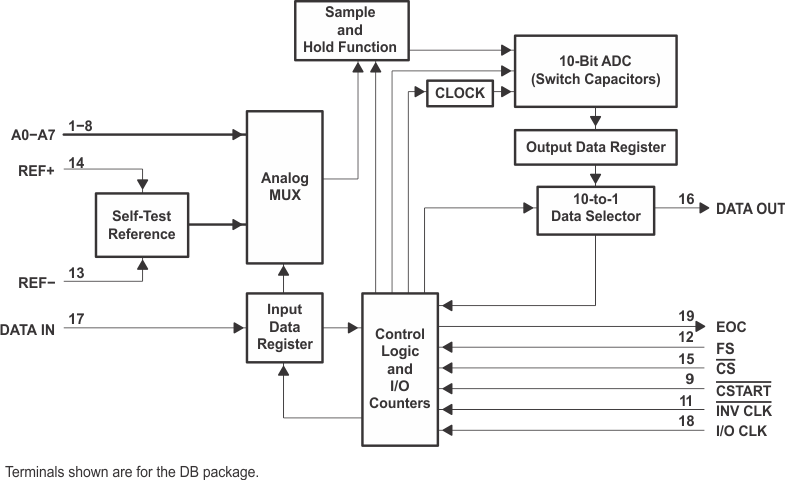
The TLV1548 is a CMOS 10-bit switched-capacitor successive-approximation (SAR) analog-to-digital (A/D) converter. The device has a chip select (CS)\, input-output clock (I/O CLK), data input (DATA IN) and serial data output (DATA OUT) that provides a direct 4-wire synchronous serial peripheral interface (SPI™, QSPI™) port of a host microprocessor. When interfacing with a TMS320 DSP, an additional frame sync signal (FS) indicates the start of a serial data frame. The device allows high-speed data transfers from the host. The INV CLK\ input provides further timing flexibility for the serial interface.In addition to a high-speed converter and versatile control capability, the device has an on-chip 11-channel multiplexer that can select any one of eight analog inputs or any one of three internal self-test voltages. The sample-and-hold function is automatic except for the extended sampling cycle, where the sampling cycle is started by the falling edge of asynchronous CSTART\. At the end of the A/D conversion, the end-of-conversion (EOC) output goes high to indicate that the conversion is complete. The TLV1548 is designed to operate with a wide range of supply voltages with very low power consumption. The power saving feature is further enhanced with a software-programmed power-down mode and conversion rate. The converter incorporated in the device features differential high-impedance reference inputs that facilitate ratiometric conversion, scaling, and isolation of analog circuitry from logic and supply noise. A switched-capacitor design allows low-error conversion over the full operating temperature range.The TLV1548 has eight analog input channels. The TLV1548Q is characterized for operation from –40°C to 125°C.
TLV1548QDBREP 数据手册
| 数据手册 | 说明 | 数量 | 操作 |
|---|---|---|---|
 TLV1548QDBREP TLV1548QDBREP
|
10 Bit Analog to Digital Converter 8 Input 1 SAR 20-SSOP |
35页,687K | 查看 |
TLV1548QDBREP 电路图
TLV1548QDBREP 电路图
TLV1548QDBREP 相关产品
- 6PADC3101TRGERQ1
- AD1674ARZ
- AD1674BRZ
- AD1674JNZ
- AD1674KRZ
- AD1974YSTZ
- AD5590BBCZ
- AD573KNZ
- AD574AJPZ
- AD574AKE
- AD574AKP
- AD574ALD
- AD574ALNZ
- AD6600ASTZ
- AD6600ASTZ-REEL
- AD6644ASTZ-40
- AD6645ASVZ-80
- AD6654CBC
- AD670JP
- AD670JPZ
- AD670JPZ-REEL7
- AD670KNZ
- AD673JNZ
- AD674BARZ
- AD674BJNZ
- AD674BKNZ
- AD676JDZ
- AD676JN
- AD676JNZ
- AD677JRZ-REEL