 搜索
搜索
 发布采购
发布采购
- 封装:64-VFQFP 裸露焊盘
- RoHS:无铅 / 符合限制有害物质指令(RoHS)规范要求
- 包装方式:托盘
- 参考价格:$10.2-$9.3
更新日期:2024-04-01 00:04:00

产品简介:用于 PON 的千兆以太网串行器/解串器
查看详情- 封装:64-VFQFP 裸露焊盘
- RoHS:无铅 / 符合限制有害物质指令(RoHS)规范要求
- 包装方式:托盘
- 参考价格:$10.2-$9.3
TLK1211RCP 供应商
- 公司
- 型号
- 品牌
- 封装/批号
- 数量
- 地区
- 日期
- 说明
- 询价
-
TI
-
原厂原装
22+ -
3288
-
上海市
-
-
-
一级代理原装
-
TI/德州仪器
-
HVQFP64
21+ -
6000
-
杭州
-
-
-
原装正品,BOM一站式服务
-
TI
-
HVQFP
2019+ -
5800
-
上海市
-
-
-
全新原装现货
-
TI/德州仪器
-
HVQFP64
10+ -
1001
-
上海市
-
-
-
原装可开发票
-
-
23+ -
46000
-
合肥
-
-
-
科大讯飞战略投资企业,提供一站式配套服务
TLK1211RCP 中文资料属性参数
- 标准包装:160
- 类别:集成电路 (IC)
- 家庭:接口 - 驱动器,接收器,收发器
- 系列:-
- 类型:收发器
- 驱动器/接收器数:1/1
- 规程:IEEE 1149.1
- 电源电压:2.3 V ~ 2.7 V
- 安装类型:表面贴装
- 封装/外壳:64-VFQFP 裸露焊盘
- 供应商设备封装:64-HVQFP
- 包装:托盘
- 其它名称:296-20780
产品特性
- 0.6-Gbps to 1.3-Gbps Serializer/Deserializer
- Low Power Consumption <250 mW (typ) at 1.25 Gbps
- Fast Relock Times Less Than 256 ns (Typ) Suitable for EPON/GEPON Applications
- LVPECL Compatible Differential I/O on High Speed Interface
- Single Monolithic PLL Design
- Support For 10-Bit Interface or Reduced Interface 5-Bit DDR (Double Data Rate) Clocking
- Receiver Differential Input Thresholds 200 mV Minimum
- IEEE 802.3 Gigabit Ethernet Compliant
- ANSI X3.230-1994 (FC-PH) Fibre Channel Compliant
- Advanced 0.25-µm CMOS Technology
- No External Filter Capacitors Required
- Comprehensive Suite of Built-In Testability
- IEEE 1149.1 JTAG Support
- 2.5-V Supply Voltage for Lowest Power Operation
- 3.3-V Tolerant on LVTTL Inputs
- Hot Plug Protection
- 64-Pin VQFP With Thermally Enhanced Package (PowerPAD)
- CPRI Data Rate Compatible (614 Mbps, 1.22 Gbps)
- Industrial Temperature Range Supported: –40°C to 85°C
产品概述
The TLK1211RCP gigabit ethernet transceiver provides for ultrahigh-speed, full-duplex, point-to-point data transmissions. This device is based on the timing requirements of the 10-bit interface specification by the IEEE 802.3 gigabit ethernet specification and is also compliant with the ANSI X3.230-1994 (FC-PH) fibre channel standard. The device supports data rates from 0.6 Gbps to 1.3 Gbps.The primary application of the transceiver is to provide building blocks for point-to-point baseband data transmission over controlled impedance media of 50 Ω. The transmission media can be printed-circuit board traces, copper cables, or fiber-optical media. The ultimate rate and distance of data transfer is dependent upon the attenuation characteristics of the media and the noise coupling to the environment.The transceiver performs the data serialization, deserialization, and clock extraction functions for a physical layer interface device. The transceiver operates at 1.25 Gbps (typical), providing up to 1 Gbps of data bandwidth over a copper or optical media interface.The transceiver supports both the defined 10-bit interface (TBI) and a reduced 5-bit interface utilizing double data rate (DDR) clocking. In the TBI mode the serializer/deserializer (SERDES) accepts 10-bit wide 8b/10b parallel encoded data bytes. The parallel data bytes are serialized and transmitted differentially at PECL compatible voltage levels. The SERDES extracts clock information from the input serial stream and deserializes the data, outputting a parallel 10-bit data byte.In the DDR mode the parallel interface accepts 5-bit wide 8b/10b encoded data aligned on both the rising and falling edges of the reference clock. The data is clocked most significant bit first (bits 0–4 of the 8b/10b encoded data) on the rising edge of the clock and the least significant bits (bits 5–9 of the 8b/10b encoded data) are clocked on the falling edge of the clock.The transceiver provides a comprehensive series of built-in tests for self-test purposes including loopback and pseudorandom binary sequence (PRBS) generation and verification. An IEEE 1149.1 JTAG port is also supported.The transceiver is housed in a high-performance, thermally enhanced, 64-pin VQFP PowerPAD package. Use of the PowerPAD package does not require any special considerations except to note that the PowerPAD, which is an exposed die pad on the bottom of the device, is a metallic thermal and electrical conductor. It is recommended that the device PowerPAD be soldered to the thermal land on the board.The transceiver is characterized for operation from –40°C to 85°C.The transceiver uses a 2.5-V supply. The I/O section is 3.3-V compatible. With a 2.5-V supply the chipset is very power-efficient, dissipating less than 250 mW typical power when operating at 1.25 Gbps. The transceiver is designed to be hot plug capable. A power-on reset causes RBC0, RBC1, the parallel output signal terminals, TXP, and TXN to be held in a high-impedance state.
TLK1211RCP 电路图
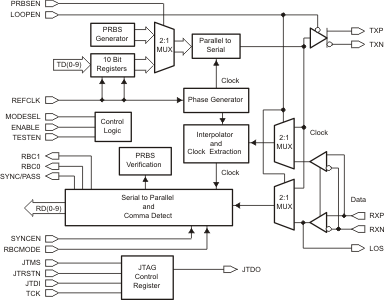
TLK1211RCP 电路图
TLK1211RCP 相关产品
- 29F52SC
- AD8016ARBZ
- AD8016ARBZ-REEL
- AD8016AREZ
- AD8016AREZ-REEL
- AD8016AREZ-REEL7
- AD8018ARUZ-REEL
- AD8018ARZ-REEL7
- AD807A-155BRZRL
- AD807A-155BRZRL7
- AD8128ACPZ-R7
- AD8145WYCPZ-R7
- AD8145YCPZ-R7
- AD8392AACPZ-RL
- AD8392AAREZ
- AD8392AAREZ-RL
- ADM1181AANZ
- ADM1385ARSZ-REEL
- ADM1385ARSZ-REEL7
- ADM1485ARMZ-REEL
- ADM1485ARMZ-REEL7
- ADM1485ARZ
- ADM1485JNZ
- ADM1486AR-REEL7
- ADM1486ARZ-REEL7
- ADM1490EBRMZ-REEL7
- ADM1490EBRZ
- ADM1490EBRZ-REEL7
- ADM202EARN-REEL
- ADM202EARNZ-REEL7