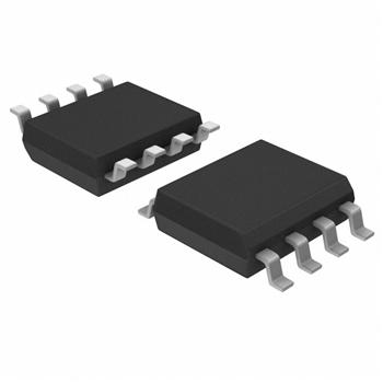
- 封装:8-SOIC(0.154",3.90mm 宽)
- RoHS:无铅 / 符合限制有害物质指令(RoHS)规范要求
- 包装方式:Digi-Reel®
- 参考价格:$1.4751-$3.16
更新日期:2024-04-01 00:04:00
产品简介:汽车类双通道低噪声高速精密运算放大器
查看详情- 封装:8-SOIC(0.154",3.90mm 宽)
- RoHS:无铅 / 符合限制有害物质指令(RoHS)规范要求
- 包装方式:Digi-Reel®
- 参考价格:$1.4751-$3.16
TLE2142QDRQ1 供应商
- 公司
- 型号
- 品牌
- 封装/批号
- 数量
- 地区
- 日期
- 说明
- 询价
-
TI
-
原厂原装
22+ -
3288
-
上海市
-
-
-
一级代理原装
-
TI/德州仪器
-
SOP8
21+ -
10000
-
杭州
-
-
-
只做原装现货,大量现货热卖
-
TI/BB
-
SOP8
新批号 -
789000
-
上海市
-
-
-
原厂发货进口原装微信同步QQ893727827
TLE2142QDRQ1 中文资料属性参数
- 标准包装:1
- 类别:集成电路 (IC)
- 家庭:Linear - Amplifiers - Instrumentation, OP Amps, Buffer Amps
- 系列:Excalibur™
- 放大器类型:通用
- 电路数:2
- 输出类型:-
- 转换速率:45 V/µs
- 增益带宽积:5.9MHz
- -3db带宽:-
- 电流 - 输入偏压:700nA
- 电压 - 输入偏移:290µV
- 电流 - 电源:6.9mA
- 电流 - 输出 / 通道:50mA
- 电压 - 电源,单路/双路(±):4 V ~ 44 V,±2 V ~ 22 V
- 工作温度:-40°C ~ 125°C
- 安装类型:表面贴装
- 封装/外壳:8-SOIC(0.154",3.90mm 宽)
- 供应商设备封装:8-SOIC
- 包装:®
- 其它名称:296-24924-6
产品特性
- Qualified for Automotive Applications
- Low Noise 10 Hz: 15 nV/Hz 1 kHz: 10.5 nV/Hz
- 10 Hz: 15 nV/Hz
- 1 kHz: 10.5 nV/Hz
- 10000-pF Load Capability
- 20-mA Short-Circuit Output Current (Min)
- 27-V/µs Slew Rate (Min)
- High Gain-Bandwidth Product: 5.9 MHz
- Single or Split Supply: 4 V to 44 V
- Fast Settling Time 340 ns to 0.1% 400 ns to 0.01%
- 340 ns to 0.1%
- 400 ns to 0.01%
- Large Output Swing: VCC– + 0.1 V to VCC+ – 1 V
产品概述
The TLE2142 device is a high-performance, internally compensated operational amplifier built using the Texas Instruments complementary bipolar Excalibur™ process. It is a pin-compatible upgrade to standard industry products.The design incorporates an input stage that simultaneously achieves low audio-band noise of 10.5 nV/Hz with a 10-Hz 1/f corner and symmetrical 40-V/µs slew rate typically with loads up to 800 pF. The resulting low distortion and high power bandwidth are important in high-fidelity audio applications. A fast settling time of 340 ns to 0.1% of a 10-V step with a 2-k/100-pF load is useful in fast actuator/positioning drivers. Under similar test conditions, settling time to 0.01% is 400 ns.The device is stable with capacitive loads up to 10 nF, although the 6-MHz bandwidth decreases to 1.8 MHz at this high loading level. As such, the TLE2142 is useful for low-droop sample-and-holds and direct buffering of long cables, including 4-mA to 20-mA current loops.The special design also exhibits an improved insensitivity to inherent integrated circuit component mismatches as is evidenced by a 500-µV maximum offset voltage and 1.7-µV/°C typical drift. Minimum common-mode rejection ratio and supply-voltage rejection ratio are
85 dB and 90 dB, respectively.Device performance is relatively independent of supply voltage over the ±2-V to ±22-V range. Inputs can operate between VCC– – 0.3 V to VCC+ – 1.8 V without inducing phase reversal, although excessive input current may flow out of each input exceeding the lower common-mode input range. The all-npn output stage provides a nearly rail-to-rail output swing of
VCC– + 0.1 V to VCC+ – 1 V under light current-loading conditions. The device can sustain shorts to either supply, because output current is internally limited, but care must be taken to ensure that maximum package power dissipation is not exceeded.The TLE2142 can also be used as a comparator. Differential inputs of VCC± can be maintained without damage to the device. Open-loop propagation delay with TTL supply levels is typically 200 ns. This gives a good indication as to output stage saturation recovery when the device is driven beyond the limits of recommended output swing.The TLE2142 device is available in industry-standard 8-pin small-outline (D) packages. The device is characterized for operation from –40°C to 125°C.
TLE2142QDRQ1 相关产品
- ACPL-7900-000E
- ACPL-7900-300E
- ACPL-790A-000E
- ACPL-790B-000E
- ACPL-790B-300E
- ACPL-C784-000E
- ACPL-C790-500E
- ACPL-C79A-500E
- ACPL-C79B-500E
- AD202JY
- AD202KN
- AD202KY
- AD210AN
- AD210BN
- AD521JDZ
- AD521KDZ
- AD521LDZ
- AD524AE
- AD524ARZ-16-REEL7
- AD524BE
- AD524CD
- AD526BDZ
- AD526CD
- AD526CDZ
- AD526JNZ
- AD526SD
- AD548JRZ-REEL
- AD548KNZ
- AD5748ACPZ-RL7
- AD5749ACPZ-RL7

 搜索
搜索
 发布采购
发布采购
