 搜索
搜索
 发布采购
发布采购
- 封装:20-DIP(0.300",7.62mm)
- RoHS:无铅 / 符合限制有害物质指令(RoHS)规范要求
- 包装方式:管件
- 参考价格:$2.6536-$5.99
更新日期:2024-04-01 00:04:00
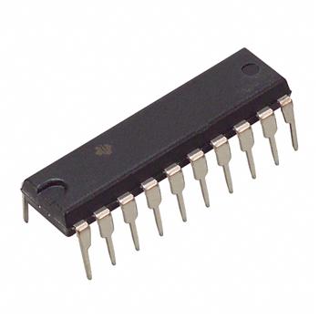
产品简介:具有并行输入、单/双电源的 8 位、5us 四通道 DAC
查看详情- 封装:20-DIP(0.300",7.62mm)
- RoHS:无铅 / 符合限制有害物质指令(RoHS)规范要求
- 包装方式:管件
- 参考价格:$2.6536-$5.99
TLC7226CN 供应商
- 公司
- 型号
- 品牌
- 封装/批号
- 数量
- 地区
- 日期
- 说明
- 询价
-
TI
-
原厂原装
22+ -
3288
-
上海市
-
-
-
一级代理原装
-
TI
-
DIP
7 -
1000
-
杭州
-
-
-
原装正品现货
-
TI/德州仪器
-
21+
DIP20 -
9862
-
杭州
-
-
-
只做原装现货,大量现货热卖
-
TI
-
-
2019+ -
5800
-
上海市
-
-
-
全新原装现货
-
TI
-
DIP
23+ -
15000
-
上海市
-
-
-
中国区代理原装现货热卖特价
-
TI
-
原厂封装
21+ -
3500
-
上海市
-
-
-
原装现货,品质为先!请来电垂询!
-
TI
-
原厂原封装
新批号 -
887000
-
上海市
-
-
-
原厂发货进口原装微信同步QQ893727827
-
TI
-
DIP
22+ -
5000
-
常州
-
-
-
全新原装现货热卖
-
TI
-
DIP20
23+ -
5800
-
上海市
-
-
-
进口原装现货,杜绝假货。
TLC7226CN 中文资料属性参数
- 产品培训模块:Data Converter Basics
- 标准包装:20
- 类别:集成电路 (IC)
- 家庭:数据采集 - 数模转换器
- 系列:-
- 设置时间:5µs,7µs
- 位数:8
- 数据接口:并联
- 转换器数目:4
- 电压电源:双 ±
- 功率耗散(最大):500mW
- 工作温度:0°C ~ 70°C
- 安装类型:通孔
- 封装/外壳:20-DIP(0.300",7.62mm)
- 供应商设备封装:20-PDIP
- 包装:管件
- 输出数目和类型:4 电压,单极;4 电压,双极
- 采样率(每秒):143k
- 其它名称:296-3018-5
产品特性
- Four 8-Bit D/A Converters
- Microprocessor Compatible
- TTL/CMOS Compatible
- Single Supply Operation Possible
- CMOS Technology
- Applications Process Control Automatic Test Equipment Automatic Calibration of Large System Parameters, e.g. Gain/Offset
- Process Control
- Automatic Test Equipment
- Automatic Calibration of Large System Parameters, e.g. Gain/Offset
产品概述
The TLC7226C, TLC7226I, and TLC7226M consist of four 8-bit voltage-output digital-to-analog converters (DACs) with output buffer amplifiers and interface logic on a single monolithic chip.Separate on-chip latches are provided for each of the four DACs. Data is transferred into one of these data latches through a common 8-bit TTL/CMOS-compatible 5-V input port. Control inputs A0 and A1 determine which DAC is loaded when WR goes low. The control logic is speed compatible with most 8-bit microprocessors.Each DAC includes an output buffer amplifier capable of sourcing up to 5 mA of output current.The TLC7226 performance is specified for input reference voltages from 2 V to VDD – 4 V with dual supplies. The voltage mode configuration of the DACs allows the TLC7226 to be operated from a single power supply rail at a reference of 10 V.The TLC7226 is fabricated in a LinBiCMOS™ process that has been specifically developed to allow high-speed digital logic circuits and precision analog circuits to be integrated on the same chip. The TLC7226 has a common 8-bit data bus with individual DAC latches. This provides a versatile control architecture for simple interface to microprocessors. All latch-enable signals are level triggered.Combining four DACs, four operational amplifiers, and interface logic into either a 0.3-inch wide, 20-terminal dual-in-line IC (DIP) or a small 20-terminal small-outline IC (SOIC) allows a dramatic reduction in board space requirements and offers increased reliability in systems using multiple converters. The Leadless Ceramic Chip Carrier (LCCC) package provides for operation at military temperature range. The pinout is aimed at optimizing board layout with all of the analog inputs and outputs at one end of the package and all of the digital inputs at the other.The TLC7226C is characterized for operation from 0°C to 70°C. The TLC7226I is characterized for operation from –25°C to 85°C. The TLC7226M is characterized for operation from –55°C to 125°C.
TLC7226CN 电路图
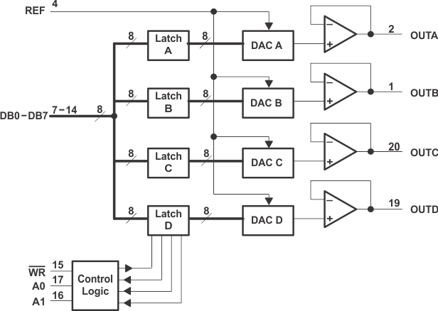
TLC7226CN 电路图
TLC7226CN 相关产品
- AD1833AASTZ
- AD1851RZ-J
- AD1851RZ-REEL7
- AD1852JRSZRL
- AD1856RZ
- AD1859JRZ-RL
- AD1866RZ-REEL
- AD1933WBSTZ
- AD1934WBSTZ
- AD1953YSTZ
- AD1954YSTZ
- AD1954YSTZRL
- AD1955ARSZ
- AD1955ARSZRL
- AD420AR-32-REEL
- AD420ARZ-32
- AD420ARZ-32-REEL
- AD421BR
- AD421BRZ
- AD421BRZRL
- AD421BRZRL7
- AD5024BRUZ
- AD5024BRUZ-REEL7
- AD5025BRUZ
- AD5040BRJZ-REEL7
- AD5044BRUZ
- AD5060ARJZ-2REEL7
- AD5060BRJZ-1500RL7
- AD5060BRJZ-1REEL7
- AD5060BRJZ-2500RL7