 搜索
搜索
 发布采购
发布采购
- 封装:8-SOIC(0.154",3.90mm 宽)
- RoHS:无铅 / 符合限制有害物质指令(RoHS)规范要求
- 包装方式:管件
- 参考价格:$9.52747
更新日期:2024-04-01 00:04:00
产品简介:12 位、串行输入、可编程稳定时间、同步更新、低功耗、2.5us 双通道 DAC
查看详情- 封装:8-SOIC(0.154",3.90mm 宽)
- RoHS:无铅 / 符合限制有害物质指令(RoHS)规范要求
- 包装方式:管件
- 参考价格:$9.52747
TLC5618AQDG4 供应商
- 公司
- 型号
- 品牌
- 封装/批号
- 数量
- 地区
- 日期
- 说明
- 询价
-
TI
-
原厂原装
22+ -
3288
-
上海市
-
-
-
一级代理原装
-
TI(德州仪器)
-
SOIC-8
2022+ -
12000
-
上海市
-
-
-
原装可开发票
TLC5618AQDG4 中文资料属性参数
- 产品培训模块:Data Converter Basics
- 标准包装:75
- 类别:集成电路 (IC)
- 家庭:数据采集 - 数模转换器
- 系列:-
- 设置时间:250ns
- 位数:12
- 数据接口:串行
- 转换器数目:2
- 电压电源:单电源
- 功率耗散(最大):3mW
- 工作温度:-40°C ~ 125°C
- 安装类型:表面贴装
- 封装/外壳:8-SOIC(0.154",3.90mm 宽)
- 供应商设备封装:8-SOIC
- 包装:管件
- 输出数目和类型:2 电压,单极
- 采样率(每秒):75k
产品特性
- Programmable Settling Time to 0.5 LSB 2.5 us or 12.5 us Typ
- Two 12-Bit CMOS Voltage Output DACs in an 8-Pin Package
- Simultaneous Updates for DAC A and DAC B
- Single Supply Operation
- 3-Wire Serial Interface
- High-Impedance Reference Inputs
- Voltage Output Range ... 2 Times the Reference Input Voltage
- Software Powerdown Mode
- Internal Power-On Reset
- TMS320 and SPI Compatible
- Low Power Consumption:
- 3 mW Typ in Slow Mode,
- 8 mW Typ in Fast Mode
- Input Data Update Rate of 1.21 MHz
- Monotonic Over Temperature
- Available in Q-Temp Automotive High Rel Automotive Applications Configuration Control/Print Support Qualification to Automotive Standards
- Applications Battery Powered Test Instruments Digital Offset and Gain Adjustment Battery Operated/Remote Industrial Controls Machine and Motion Control Devices Cellular Telephones
- Battery Powered Test Instruments
- Digital Offset and Gain Adjustment
- Battery Operated/Remote Industrial Controls
- Machine and Motion Control Devices
- Cellular Telephones
产品概述
The TLC5618 is a dual 12-bit voltage output digital-to-analog converter (DAC) with buffered reference inputs (high impedance). The DACs
have an output voltage range that is two times the reference voltage, and the DACs are monotonic. The device is simple to use, running from a single
supply of 5 V. A power-on reset function is incorporated in the device to ensure repeatable start-up conditions.
Digital control of the TLC5618 is over a 3-wire CMOS-compatible serial bus. The device receives a 16-bit word for programming and
producing the analog output. The digital inputs feature Schmitt triggers for high noise immunity. Digital communication protocols include the
SPI™, QSPI™, and Microwire™ standards.
Two versions of the device are available. The TLC5618 does not have an internal state machine and is dependent on all external timing signals. The TLC5618A has an internal state machine that counts the
number of clocks from the falling edge of CS\ and then updates and disables the device from accepting further
data inputs. The TLC5618A is recommended for TMS320 and SPI processors, and the TLC5618 is
recommended only for SPI or 3-wire serial port processors. The TLC5618A is backward-compatible and
designed to work in TLC5618 designed systems.
The 8-terminal small-outline D package allows digital control of analog functions in space-critical applications.
The TLC5618C is characterized for operation from 0°C to 70°C. The TLC5618I is characterized for operation
from \x9640°C to 85°C. The TLC5618Q is characterized for operation from \x9640°C to 125°C. The TLC5618M is
characterized for operation from \x9655°C to 125°C.
TLC5618AQDG4 电路图
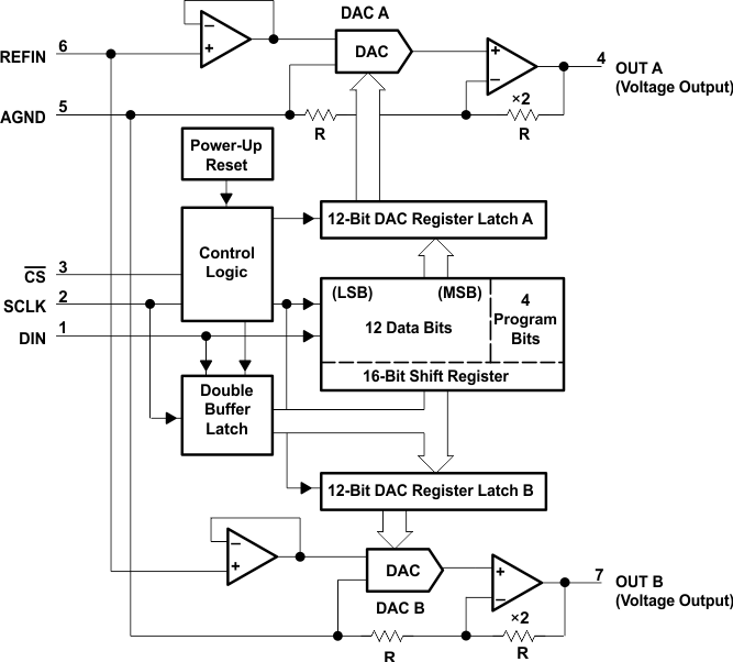
TLC5618AQDG4 电路图
TLC5618AQDG4 相关产品
- AD1833AASTZ
- AD1851RZ-J
- AD1851RZ-REEL7
- AD1852JRSZRL
- AD1856RZ
- AD1859JRZ-RL
- AD1866RZ-REEL
- AD1933WBSTZ
- AD1934WBSTZ
- AD1953YSTZ
- AD1954YSTZ
- AD1954YSTZRL
- AD1955ARSZ
- AD1955ARSZRL
- AD420AR-32-REEL
- AD420ARZ-32
- AD420ARZ-32-REEL
- AD421BR
- AD421BRZ
- AD421BRZRL
- AD421BRZRL7
- AD5024BRUZ
- AD5024BRUZ-REEL7
- AD5025BRUZ
- AD5040BRJZ-REEL7
- AD5044BRUZ
- AD5060ARJZ-2REEL7
- AD5060BRJZ-1500RL7
- AD5060BRJZ-1REEL7
- AD5060BRJZ-2500RL7