 搜索
搜索
 发布采购
发布采购
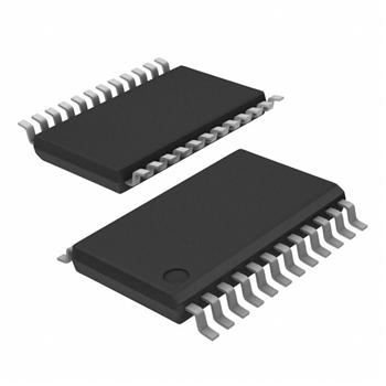
- 封装:24-TSSOP(0.173",4.40mm 宽)
- RoHS:无铅 / 符合限制有害物质指令(RoHS)规范要求
- 包装方式:带卷 (TR)
- 参考价格:$3.126
更新日期:2024-04-01 00:04:00
产品简介:具有 2Vpp 输入的 8 位 20MSPS 模数转换器 (ADC)
查看详情- 封装:24-TSSOP(0.173",4.40mm 宽)
- RoHS:无铅 / 符合限制有害物质指令(RoHS)规范要求
- 包装方式:带卷 (TR)
- 参考价格:$3.126
TLC5510IPWR 供应商
- 公司
- 型号
- 品牌
- 封装/批号
- 数量
- 地区
- 日期
- 说明
- 询价
-
TI
-
原厂原装
22+ -
3288
-
上海市
-
-
-
一级代理原装
-
TI
-
TSSOP-24
10+ -
2909
-
杭州
-
-
-
原装正品现货
-
TI/德州仪器
-
TSSOP24
21+ -
10000
-
杭州
-
-
-
只做原装现货,大量现货热卖
-
TI
-
SOP20
23+ -
15000
-
上海市
-
-
-
中国区代理原装现货热卖特价
-
TI
-
-
21+ -
9000
-
上海市
-
-
-
原装现货,品质为先!请来电垂询!
-
TI
-
TSSOP24
新批号 -
8877000
-
上海市
-
-
-
原厂发货进口原装微信同步QQ893727827
-
TI
-
TSSOP
23+ -
5800
-
上海市
-
-
-
进口原装现货,杜绝假货。
TLC5510IPWR 中文资料属性参数
- 产品培训模块:Data Converter Basics
- 标准包装:2,000
- 类别:集成电路 (IC)
- 家庭:数据采集 - 模数转换器
- 系列:-
- 位数:8
- 采样率(每秒):20M
- 数据接口:并联
- 转换器数目:1
- 功率耗散(最大):127.5mW
- 电压电源:模拟和数字
- 工作温度:-20°C ~ 75°C
- 安装类型:表面贴装
- 封装/外壳:24-TSSOP(0.173",4.40mm 宽)
- 供应商设备封装:24-TSSOP
- 包装:带卷 (TR)
- 输入数目和类型:1 个单端,单极
- 配用:296-10332-ND - EVAL MOD FOR TLC5510
产品特性
- Analog Input Range TLC5510...2 V Full Scale TLC5510A...4 V Full Scale
- TLC5510...2 V Full Scale
- TLC5510A...4 V Full Scale
- 8-Bit Resolution
- Integral Linearity Error ±0.75 LSB Max (25°C) ±1 LSB Max (–20°C to 75°C)
- Differential Linearity Error ±0.5 LSB Max (25°C) ±0.75 LSB Max (–20°C to 75°C)
- Maximum Conversion Rate 20 Mega-Samples per Second (MSPS) Max
- 5-V Single-Supply Operation
- Low Power Consumption TLC5510...127.5 mW Typ TLC5510A...150 mW Typ (includes reference resistor dissipation)
- TLC5510 is Interchangeable With Sony CXD1175
- applications Digital TV Medical Imaging Video Conferencing High-Speed Data Conversion QAM Demodulators
- Digital TV
- Medical Imaging
- Video Conferencing
- High-Speed Data Conversion
- QAM Demodulators
产品概述
The TLC5510 and TLC5510A are CMOS, 8-bit, 20 MSPS analog-to-digital converters (ADCs) that utilize a semiflash architecture. The TLC5510 and TLC5510A operate with a single 5-V supply and typically consume only 130 mW of power. Included is an internal sample-and-hold circuit, parallel outputs with high-impedance mode, and internal reference resistors.The semiflash architecture reduces power consumption and die size compared to flash converters. By implementing the conversion in a 2-step process, the number of comparators is significantly reduced. The latency of the data output valid is 2.5 clocks.The TLC5510 uses the three internal reference resistors to create a standard, 2-V, full-scale conversion range using VDDA. Only external jumpers are required to implement this option and eliminates the need for external reference resistors. The TLC5510A uses only the center internal resistor section with an externally applied 4-V reference such that a 4-V input signal can be used. Differential linearity is 0.5 LSB at 25°C and a maximum of 0.75 LSB over the full operating temperature range. Typical dynamic specifications include a differential gain of 1% and differential phase of 0.7 degrees.The TLC5510 and TLC5510A are characterized for operation from -20°C to 75°C.
TLC5510IPWR 相关产品
- 6PADC3101TRGERQ1
- AD1674ARZ
- AD1674BRZ
- AD1674JNZ
- AD1674KRZ
- AD1974YSTZ
- AD5590BBCZ
- AD573KNZ
- AD574AJPZ
- AD574AKE
- AD574AKP
- AD574ALD
- AD574ALNZ
- AD6600ASTZ
- AD6600ASTZ-REEL
- AD6644ASTZ-40
- AD6645ASVZ-80
- AD6654CBC
- AD670JP
- AD670JPZ
- AD670JPZ-REEL7
- AD670KNZ
- AD673JNZ
- AD674BARZ
- AD674BJNZ
- AD674BKNZ
- AD676JDZ
- AD676JN
- AD676JNZ
- AD677JRZ-REEL