 搜索
搜索
 发布采购
发布采购
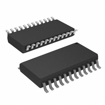
- 封装:24-SOIC(0.295",7.50mm 宽)
- RoHS:无铅 / 符合限制有害物质指令(RoHS)规范要求
- 包装方式:带卷 (TR)
- 参考价格:$5.513
更新日期:2024-04-01 00:04:00
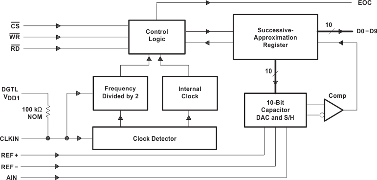
产品简介:与 DSP/微处理器直接相连的 10 位、164kSPS 并行输出 ADC
查看详情- 封装:24-SOIC(0.295",7.50mm 宽)
- RoHS:无铅 / 符合限制有害物质指令(RoHS)规范要求
- 包装方式:带卷 (TR)
- 参考价格:$5.513
TLC1550IDWR 供应商
- 公司
- 型号
- 品牌
- 封装/批号
- 数量
- 地区
- 日期
- 说明
- 询价
-
TI
-
原厂原装
22+ -
3288
-
上海市
-
-
-
一级代理原装
TLC1550IDWR 中文资料属性参数
- 产品培训模块:Data Converter Basics
- 标准包装:2,000
- 类别:集成电路 (IC)
- 家庭:数据采集 - 模数转换器
- 系列:-
- 位数:10
- 采样率(每秒):164k
- 数据接口:并联
- 转换器数目:1
- 功率耗散(最大):40mW
- 电压电源:模拟和数字
- 工作温度:-40°C ~ 85°C
- 安装类型:表面贴装
- 封装/外壳:24-SOIC(0.295",7.50mm 宽)
- 供应商设备封装:24-SOIC
- 包装:带卷 (TR)
- 输入数目和类型:1 个单端,单极
产品特性
- Power Dissipation...40 mW Max
- Advanced LinEPIC™ Single-Poly Process Provides Close Capacitor Matching for Better Accuracy
- Fast Parallel Processing for DSP and µP Interface
- Either External or Internal Clock Can Be Used
- Conversion Time...6 µs
- Total Unadjusted Error...±1 LSB Max
- CMOS Technology
产品概述
The TLC1550x and TLC1551 are data acquisition analog-to-digital converters (ADCs) using a 10-bit, switched-capacitor, successive-approximation network. A high-speed, 3-state parallel port directly interfaces to a digital signal processor (DSP) or microprocessor (µP) system data bus. D0 through D9 are the digital output terminals with D0 being the least significant bit (LSB). Separate power terminals for the analog and digital portions minimize noise pickup in the supply leads. Additionally, the digital power is divided into two parts to separate the lower current logic from the higher current bus drivers. An external clock can be applied to CLKIN to override the internal system clock if desired.The TLC1550I and TLC1551I are characterized for operation from –40°C to 85°C. The TLC1550M is characterized over the full military range of –55°C to 125°C.
TLC1550IDWR 电路图
TLC1550IDWR 电路图
TLC1550IDWR 相关产品
- 6PADC3101TRGERQ1
- AD1674ARZ
- AD1674BRZ
- AD1674JNZ
- AD1674KRZ
- AD1974YSTZ
- AD5590BBCZ
- AD573KNZ
- AD574AJPZ
- AD574AKE
- AD574AKP
- AD574ALD
- AD574ALNZ
- AD6600ASTZ
- AD6600ASTZ-REEL
- AD6644ASTZ-40
- AD6645ASVZ-80
- AD6654CBC
- AD670JP
- AD670JPZ
- AD670JPZ-REEL7
- AD670KNZ
- AD673JNZ
- AD674BARZ
- AD674BJNZ
- AD674BKNZ
- AD676JDZ
- AD676JN
- AD676JNZ
- AD677JRZ-REEL