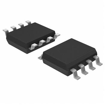
- 封装:8-SOIC(0.154",3.90mm 宽)
- RoHS:无铅 / 符合限制有害物质指令(RoHS)规范要求
- 包装方式:带卷 (TR)
- 参考价格:$3.032
更新日期:2024-04-01 00:04:00
产品简介:双路微功耗精密低电压运算放大器
查看详情- 封装:8-SOIC(0.154",3.90mm 宽)
- RoHS:无铅 / 符合限制有害物质指令(RoHS)规范要求
- 包装方式:带卷 (TR)
- 参考价格:$3.032
TLC1078IDR 供应商
- 公司
- 型号
- 品牌
- 封装/批号
- 数量
- 地区
- 日期
- 说明
- 询价
-
TI
-
原厂原装
22+ -
3288
-
上海市
-
-
-
一级代理原装
-
TI/德州仪器
-
SOIC8
21+ -
6000
-
杭州
-
-
-
原装正品,BOM一站式服务
-
TI(德州仪器)
-
SOIC-8
2022+ -
12000
-
上海市
-
-
-
原装可开发票
TLC1078IDR 中文资料属性参数
- 标准包装:2,500
- 类别:集成电路 (IC)
- 家庭:Linear - Amplifiers - Instrumentation, OP Amps, Buffer Amps
- 系列:LinCMOS™
- 放大器类型:通用
- 电路数:2
- 输出类型:-
- 转换速率:0.047 V/µs
- 增益带宽积:110kHz
- -3db带宽:-
- 电流 - 输入偏压:0.7pA
- 电压 - 输入偏移:180µV
- 电流 - 电源:29µA
- 电流 - 输出 / 通道:30mA
- 电压 - 电源,单路/双路(±):3 V ~ 16 V
- 工作温度:-40°C ~ 85°C
- 安装类型:表面贴装
- 封装/外壳:8-SOIC(0.154",3.90mm 宽)
- 供应商设备封装:8-SOIC
- 包装:带卷 (TR)
产品特性
- Power Dissipation as Low as 10 uW Typ Per Amplifier
- Operates on a Single Silver-Oxide Watch Battery, VDD = 1.4 V Min
- VIO...450 uV/850 uV Max in DIP and Small-Outline Package (TLC1078/79)
- Input Offset Voltage Drift...0.1 uV/Month Typ, Including the First 30 Days
- High-impedance LinCMOSTM Inputs
- IIB = 0.6 pA Typ
- High Open-Loop Gain...800000 Typ
- Output Drive Capability > 20 mA
- Slew Rate...47 V/ms Typ
- Common-Mode Input Voltage Range Extends Below the Negative Rail
- Output Voltage Range Includes Negative Rail
- On-Chip ESD-Protection Circuitry
- Small-Outline Package Option Also Available in Tape and Reel
产品概述
The TLC107x operational amplifiers offer ultra-low offset voltage, high gain, 110-kHz bandwidth, 47-V/ms slew rate, and just 150-uW power dissipation per amplifier.
With a supply voltage of 1.4 V, common-mode input to the negative rail, and output swing to the negative rail, the TLC107xC is an ideal solution for low-voltage battery-operated systems. The 20-mA output drive capability means that the TLC107x can easily drive small resistive and large capacitive loads when needed, while maintaining ultra-low standby power dissipation.
Since this device is functionally compatible as well as pin compatible with the TLC27L2/4 and TLC27L7/9, the TLC107x easily upgrades existing designs that can benefit from its improved performance.
The TLC107x incorporates internal ESD-protection circuits that will prevent functional failures at voltages up to 2000 V as tested under MIL-PRF-38535, Method 3015.2; however, care should be exercised when handling these devices as exposure to ESD may result in degradation of the device parametric performance. The TLC107x design also inhibits latch-up of the device inputs and outputs even with surge currents as large 100 mA.
The C-suffix devices are characterized for operation from 0°C to 70°C. The I-suffix devices are characterized for operation from -40°C to 85°C. The M-suffix devices are characterized for operation over the full military temperature range of -55°C to 125°C. The wide range of packaging options includes small-outline and chip-carrier versions for high-density system applications.
TLC1078IDR 相关产品
- ACPL-7900-000E
- ACPL-7900-300E
- ACPL-790A-000E
- ACPL-790B-000E
- ACPL-790B-300E
- ACPL-C784-000E
- ACPL-C790-500E
- ACPL-C79A-500E
- ACPL-C79B-500E
- AD202JY
- AD202KN
- AD202KY
- AD210AN
- AD210BN
- AD521JDZ
- AD521KDZ
- AD521LDZ
- AD524AE
- AD524ARZ-16-REEL7
- AD524BE
- AD524CD
- AD526BDZ
- AD526CD
- AD526CDZ
- AD526JNZ
- AD526SD
- AD548JRZ-REEL
- AD548KNZ
- AD5748ACPZ-RL7
- AD5749ACPZ-RL7

 搜索
搜索
 发布采购
发布采购
