 搜索
搜索
 发布采购
发布采购
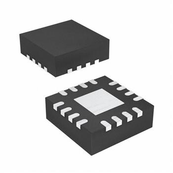
- 封装:16-VFQFN 裸露焊盘
- RoHS:无铅 / 符合限制有害物质指令(RoHS)规范要求
- 包装方式:带卷 (TR)
- 参考价格:$4.875
更新日期:2024-04-01 00:04:00
产品简介:1.9GHz、宽带、低噪声、低失真、全差分放大器
查看详情- 封装:16-VFQFN 裸露焊盘
- RoHS:无铅 / 符合限制有害物质指令(RoHS)规范要求
- 包装方式:带卷 (TR)
- 参考价格:$4.875
THS4509RGTR 供应商
- 公司
- 型号
- 品牌
- 封装/批号
- 数量
- 地区
- 日期
- 说明
- 询价
-
TI
-
原厂原装
22+ -
3288
-
上海市
-
-
-
一级代理原装
-
TI/德州仪器
-
QFN
21+ -
11855
-
杭州
-
-
-
只做原装现货,大量现货热卖
-
TI(德州仪器)
-
QFN-16(3x3)
2022+ -
12000
-
上海市
-
-
-
原装可开发票
-
TI
-
原厂原封装
新批号 -
887000
-
上海市
-
-
-
原厂发货进口原装微信同步QQ893727827
THS4509RGTR 中文资料属性参数
- 标准包装:3,000
- 类别:集成电路 (IC)
- 家庭:Linear - Amplifiers - Instrumentation, OP Amps, Buffer Amps
- 系列:-
- 放大器类型:差分
- 电路数:1
- 输出类型:差分
- 转换速率:6600 V/µs
- 增益带宽积:3GHz
- -3db带宽:2GHz
- 电流 - 输入偏压:8µA
- 电压 - 输入偏移:1000µV
- 电流 - 电源:37.7mA
- 电流 - 输出 / 通道:96mA
- 电压 - 电源,单路/双路(±):3 V ~ 5.25 V,±1.5 V ~ 2.625 V
- 工作温度:-40°C ~ 85°C
- 安装类型:表面贴装
- 封装/外壳:16-VFQFN 裸露焊盘
- 供应商设备封装:16-QFN-EP(3x3)
- 包装:带卷 (TR)
- 配用:296-31387-ND - EVAL MODULE FOR THS4520296-21087-ND - EVALUATION MODULE FOR THS4513296-21086-ND - EVALUATION MODULE FOR THS4511296-21085-ND - EVALUATION MODULE FOR THS4508296-18855-ND - EVAL MODULE FOR THS4509
产品特性
- Fully-Differential Architecture
- Centered Input Common-Mode Range
- Output Common-Mode Control
- Minimum Gain of 2 V/V (6 dB)
- Bandwidth: 1900 MHz
- Slew Rate: 6600 V/µs
- 1% Settling Time: 2 ns
- HD2: –75 dBc at 100 MHz
- HD3: –80 dBc at 100 MHz
- OIP3: 37 dBm at 70 MHz
- Input Voltage Noise: 1.9 nV/√Hz (f > 10 MHz)
- Power-Supply Voltage: 3 V to 5 V
- Power-Supply Current: 37.7 mA
- Power-Down Current: 0.65 mA
- APPLICATIONS 5-V Data Acquisition Systems High Linearity ADC Amplifiers Wireless Communication Medical Imaging Test and Measurement
- 5-V Data Acquisition Systems High Linearity ADC Amplifiers
- Wireless Communication
- Medical Imaging
- Test and Measurement
产品概述
The THS4509 device is a wideband, fully-differential op amp designed for 5-V data
acquisition systems. It has a low noise at 1.9 nV/√Hz, and low harmonic
distortion of –75 dBc HD2 and –80 dBc HD3 at 100 MHz
with 2 VPP, G = 10 dB, and 1-kΩ load. Slew rate is high at 6600 V/µs, and
with settling time of 2 ns to 1% (2-V step), it is ideal for pulsed applications. It is designed
for a minimum gain of 6 dB, but is optimized for gains of 10 dB.To allow for DC coupling to analog-to-digital converters (ADCs), its unique output
common-mode control circuit maintains the output common-mode voltage within 3-mV offset (typical)
from the set voltage, when set within 0.5-V of midsupply, with less than 4-mV differential offset
voltage. The common-mode set point is set to midsupply by internal circuitry, which may be
overdriven from an external source.The input and output are optimized for best performance with the common-mode voltages set
to midsupply. Along with high performance at low power-supply voltage, this design makes it ideal
for high-performance, single-supply 5-V data acquisition systems. The combined performance of the
THS4509 in a gain of 10 dB driving the ADS5500 ADC, sampling at 125 MSPS, is 81-dBc SFDR
and 69.1-dBc SNR with a –1 dBFS signal at 70 MHz.The THS4509 is offered in a quad, leadless VQFN-16 package (RGT), and is characterized
for operation over the full industrial temperature range from –40°C to +85°C.
THS4509RGTR 电路图
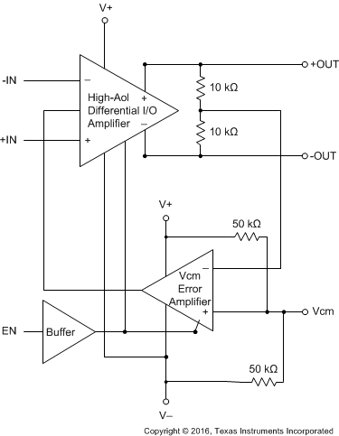
THS4509RGTR 电路图
THS4509RGTR 相关产品
- ACPL-7900-000E
- ACPL-7900-300E
- ACPL-790A-000E
- ACPL-790B-000E
- ACPL-790B-300E
- ACPL-C784-000E
- ACPL-C790-500E
- ACPL-C79A-500E
- ACPL-C79B-500E
- AD202JY
- AD202KN
- AD202KY
- AD210AN
- AD210BN
- AD521JDZ
- AD521KDZ
- AD521LDZ
- AD524AE
- AD524ARZ-16-REEL7
- AD524BE
- AD524CD
- AD526BDZ
- AD526CD
- AD526CDZ
- AD526JNZ
- AD526SD
- AD548JRZ-REEL
- AD548KNZ
- AD5748ACPZ-RL7
- AD5749ACPZ-RL7