 搜索
搜索
 发布采购
发布采购
- 封装:32-TSSOP(0.240",6.10mm 宽)
- RoHS:无铅 / 符合限制有害物质指令(RoHS)规范要求
- 包装方式:带卷 (TR)
- 参考价格:$10.969
更新日期:2024-04-01 00:04:00

产品简介:12 位、6MSPS ADC,四通道(可配置)、DSP/uP 接口、集成16x FIFO、信道自动扫描功能和低功耗模式
查看详情- 封装:32-TSSOP(0.240",6.10mm 宽)
- RoHS:无铅 / 符合限制有害物质指令(RoHS)规范要求
- 包装方式:带卷 (TR)
- 参考价格:$10.969
THS1206CDAR 供应商
- 公司
- 型号
- 品牌
- 封装/批号
- 数量
- 地区
- 日期
- 说明
- 询价
-
TI
-
原厂原装
22+ -
3288
-
上海市
-
-
-
一级代理原装
-
TI(德州仪器)
-
TSSOP-32
2022+ -
12000
-
上海市
-
-
-
原装可开发票
THS1206CDAR 中文资料属性参数
- 产品培训模块:Data Converter Basics
- 标准包装:2,000
- 类别:集成电路 (IC)
- 家庭:数据采集 - 模数转换器
- 系列:-
- 位数:12
- 采样率(每秒):6M
- 数据接口:并联
- 转换器数目:5
- 功率耗散(最大):600mW
- 电压电源:模拟和数字
- 工作温度:0°C ~ 70°C
- 安装类型:表面贴装
- 封装/外壳:32-TSSOP(0.240",6.10mm 宽)
- 供应商设备封装:32-TSSOP
- 包装:带卷 (TR)
- 输入数目和类型:1 个差分,单极
- 配用:296-16737-ND - EVALUATION MODULE FOR THS1206M
产品特性
- High-Speed 6 MSPS ADC
- 4 Analog Inputs
- Simultaneous Sampling of 4 Single-Ended Signals or 2 Differential Signals or Combination of Both
- Differential Nonlinearity Error: ±1 LSB
- Integral Nonlinearity Error: ±1.5 LSB
- Signal-to-Noise and Distortion Ratio: 68 dB at fI = 2 MHz
- Auto-Scan Mode for 2, 3, or 4 Inputs
- 3-V or 5-V Digital Interface Compatible
- Low Power: 216 mW Max
- 5-V Analog Single Supply Operation
- Internal Voltage References ...50 PPM/°C and ±5% Accuracy
- Glueless DSP Interface
- Parallel µC/DSP Interface
- Integrated FIFO
- Available in TSSOP Package
- Pin Compatible Upgrade to THS10064
- APPLICATIONS Radar Applications Communications Control Applications High-Speed DSP Front-End Automotive Applications
- Radar Applications
- Communications
- Control Applications
- High-Speed DSP Front-End
- Automotive Applications
产品概述
The THS1206 is a CMOS, low-power, 12-bit, 6 MSPS analog-to-digital converter (ADC). The speed, resolution, bandwidth, and single-supply operation are suited for applications in radar, imaging, high-speed acquisition, and communications. A multistage pipelined architecture with output error correction logic provides for no missing codes over the full operating temperature range. Internal control registers are used to program the ADC into the desired mode. The THS1206 consists of four analog inputs, which are sampled simultaneously. These inputs can be selected individually and configured to single-ended or differential inputs. An integrated 16 word deep FIFO allows the storage of data in order to take the load off of the processor connected to the ADC. Internal reference voltages for the ADC (1.5 V and 3.5 V) are provided.An external reference can also be chosen to suit the dc accuracy and temperature drift requirements of the application. Two different conversion modes can be selected. In single conversion mode, a single and simultaneous conversion of up to four inputs can be initiated by using the single conversion start signal (CONVST)\. The conversion clock in single conversion mode is generated internally using a clock oscillator circuit. In continuous conversion mode, an external clock signal is applied to the CONV_CLK input of the THS1206. The internal clock oscillator is switched off in continuous conversion mode.The THS1206C is characterized for operation from 0°C to 70°C, the THS1206I is characterized for operation from –40°C to 85°C, the THS1206Q is characterized to meet the rigorous requirements of the automotive environment from –40°C to 125°C, and the THS1206M is characterized for operation over the full military temperature range of –55°C to 125°C.
THS1206CDAR 电路图
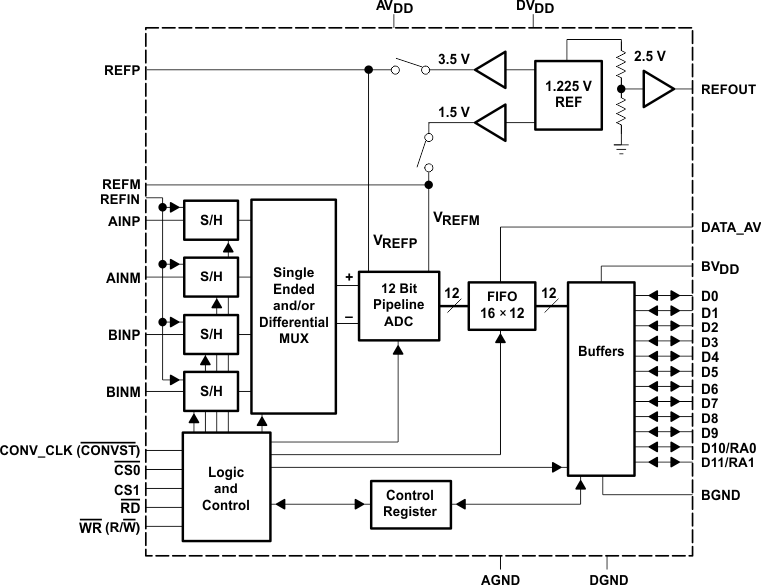
THS1206CDAR 电路图
THS1206CDAR 相关产品
- 6PADC3101TRGERQ1
- AD1674ARZ
- AD1674BRZ
- AD1674JNZ
- AD1674KRZ
- AD1974YSTZ
- AD5590BBCZ
- AD573KNZ
- AD574AJPZ
- AD574AKE
- AD574AKP
- AD574ALD
- AD574ALNZ
- AD6600ASTZ
- AD6600ASTZ-REEL
- AD6644ASTZ-40
- AD6645ASVZ-80
- AD6654CBC
- AD670JP
- AD670JPZ
- AD670JPZ-REEL7
- AD670KNZ
- AD673JNZ
- AD674BARZ
- AD674BJNZ
- AD674BKNZ
- AD676JDZ
- AD676JN
- AD676JNZ
- AD677JRZ-REEL