 搜索
搜索
 发布采购
发布采购
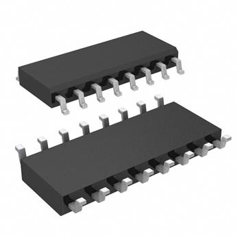
- 封装:16-SOIC(0.295",7.50mm 宽)
- RoHS:无铅 / 符合限制有害物质指令(RoHS)规范要求
- 包装方式:管件
- 参考价格:$10.38-$19.03
更新日期:2024-04-01 00:04:00
产品简介:5V 双路全双工 PECL 收发器
查看详情- 封装:16-SOIC(0.295",7.50mm 宽)
- RoHS:无铅 / 符合限制有害物质指令(RoHS)规范要求
- 包装方式:管件
- 参考价格:$10.38-$19.03
TB5T1DW 供应商
- 公司
- 型号
- 品牌
- 封装/批号
- 数量
- 地区
- 日期
- 说明
- 询价
-
TI
-
原厂原装
22+ -
3288
-
上海市
-
-
-
一级代理原装
-
TI(德州仪器)
-
SOIC-16
2022+ -
12000
-
上海市
-
-
-
原装可开发票
-
TI
-
TSSOP
23+ -
46000
-
合肥
-
-
-
科大讯飞战略投资企业,提供一站式配套服务
TB5T1DW 中文资料属性参数
- 标准包装:40
- 类别:集成电路 (IC)
- 家庭:接口 - 驱动器,接收器,收发器
- 系列:-
- 类型:收发器
- 驱动器/接收器数:2/2
- 规程:-
- 电源电压:4.5 V ~ 5.5 V
- 安装类型:表面贴装
- 封装/外壳:16-SOIC(0.295",7.50mm 宽)
- 供应商设备封装:16-SOIC
- 包装:管件
- 其它名称:296-16690-5
产品特性
- Functional Replacement for the Agere BTF1A
- Driver Features Third-State Logic Low Output ESD Protection HBM > 3 kV, CDM > 2 kV No Line Loading when VCC = 0 Capable of Driving 50- loads 2.0-ns Maximum Propagation Delay 0.2-ns Output Skew (typical)
- Third-State Logic Low Output
- ESD Protection HBM > 3 kV, CDM > 2 kV
- No Line Loading when VCC = 0
- Capable of Driving 50- loads
- 2.0-ns Maximum Propagation Delay
- 0.2-ns Output Skew (typical)
- Receiver Features High-Input Impedance Approximately 8 k 4.0-ns Maximum Propagation Delay 50-mV Hysteresis Slew Rate Limited (1 ns min 80% to 20%) ESD Protection HBM > 3 kV, CDM > 2 kV -1.1-V to 7.1-V Input Voltage Range
- High-Input Impedance Approximately 8 k
- 4.0-ns Maximum Propagation Delay
- 50-mV Hysteresis
- Slew Rate Limited (1 ns min 80% to 20%)
- ESD Protection HBM > 3 kV, CDM > 2 kV
- -1.1-V to 7.1-V Input Voltage Range
- Common Device Features Common Enable for Each Driver/Receiver Pair Operating Temperature Range: -40°C to 85°C Single 5.0 V ± 10% Supply Available in Gull-Wing SOIC (JEDEC MS-013, DW) and SOIC (D) Package
- Common Enable for Each Driver/Receiver Pair
- Operating Temperature Range: -40°C to 85°C
- Single 5.0 V ± 10% Supply
- Available in Gull-Wing SOIC (JEDEC MS-013, DW) and SOIC (D) Package
产品概述
The TB5T1 device is a dual differential driver/receiver circuit that transmits and receives digital data over balanced transmission lines. The dual drivers translate input TTL logic levels to differential pseudo-ECL output levels. The dual receivers convert differential-input logic levels to TTL output levels. Each driver or receiver pair has its own common enable control allowing serial data and a control clock to be transmitted and received on a single integrated circuit. The TB5T1 requires the customer to supply termination resistors on the circuit board.The power-down loading characteristics of the receiver input circuit are approximately 8 k relative to the power supplies; hence, it does not load the transmission line when the circuit is powered down. In circuits with termination resistors, the line remains impedance- matched when the circuit is powered down. The driver does not load the line when it is powered down.All devices are characterized for operation from -40°C to 85°C.The logic inputs of this device include internal pull-up resistors of approximately 40 k that are connected to VCC to ensure a logical high level input if the inputs are open circuited.
TB5T1DW 数据手册
| 数据手册 | 说明 | 数量 | 操作 |
|---|---|---|---|
 TB5T1DW TB5T1DW
|
DUAL DIFFERENTIAL PECL DRIVER/RECEIVER |
17 Pages页,438K | 查看 |
|
TB5T1DW
|
2/2 Transceiver Full 16-SOIC |
22页,996K | 查看 |
|
TB5T1DWE4
|
5V Dual Full-Duplex PECL Transceiver 16-SOIC -40 to 85 |
19页,617K | 查看 |
|
TB5T1DWR
|
DUAL DIFFERENTIAL PECL DRIVER/RECEIVER |
17 Pages页,438K | 查看 |
|
TB5T1DWRE4
|
5V Dual Full-Duplex PECL Transceiver 16-SOIC -40 to 85 |
19页,617K | 查看 |
TB5T1DW 相关产品
- 29F52SC
- AD8016ARBZ
- AD8016ARBZ-REEL
- AD8016AREZ
- AD8016AREZ-REEL
- AD8016AREZ-REEL7
- AD8018ARUZ-REEL
- AD8018ARZ-REEL7
- AD807A-155BRZRL
- AD807A-155BRZRL7
- AD8128ACPZ-R7
- AD8145WYCPZ-R7
- AD8145YCPZ-R7
- AD8392AACPZ-RL
- AD8392AAREZ
- AD8392AAREZ-RL
- ADM1181AANZ
- ADM1385ARSZ-REEL
- ADM1385ARSZ-REEL7
- ADM1485ARMZ-REEL
- ADM1485ARMZ-REEL7
- ADM1485ARZ
- ADM1485JNZ
- ADM1486AR-REEL7
- ADM1486ARZ-REEL7
- ADM1490EBRMZ-REEL7
- ADM1490EBRZ
- ADM1490EBRZ-REEL7
- ADM202EARN-REEL
- ADM202EARNZ-REEL7