 搜索
搜索
 发布采购
发布采购
- 封装:56-TFSOP(0.240",6.10mm 宽)
- RoHS:无铅 / 符合限制有害物质指令(RoHS)规范要求
- 包装方式:管件
- 参考价格:$3.8745-$7.88
更新日期:2024-04-01 00:04:00
产品简介:10MHz 至 135MHz、28 位 LVDS 变送器/串行器与 FlatLink? 集成电路
查看详情- 封装:56-TFSOP(0.240",6.10mm 宽)
- RoHS:无铅 / 符合限制有害物质指令(RoHS)规范要求
- 包装方式:管件
- 参考价格:$3.8745-$7.88
SN75LVDS83BDGG 供应商
- 公司
- 型号
- 品牌
- 封装/批号
- 数量
- 地区
- 日期
- 说明
- 询价
-
SN75LVDS83BDGG
原装现货 -
TI
-
TSSOP56
20+ -
10000
-
深圳
-
12-10
-
助力国营二十余载,一站式解决BOM配单,行业标杆企
-
TI
-
TSSOP56
23+ -
10990
-
上海市
-
-
-
原装优势品牌
-
TI
-
TSSOP
23+ -
5800
-
上海市
-
-
-
进口原装现货,杜绝假货。
-
TI
-
TSSOP
23+ -
46000
-
合肥
-
-
-
科大讯飞战略投资企业,提供一站式配套服务
-
TI
-
TSSOP-56
21+ -
10000
-
上海市
-
-
-
原装现货,品质为先,请来电垂询!
-
TI
-
TSSOP56
22+ -
300000
-
常州
-
-
-
原装正品
-
TI
-
TSSOP-56
10+ -
2576
-
杭州
-
-
-
原装正品现货
-
TI/德州仪器
-
TSSOP56
21+ -
10000
-
杭州
-
-
-
只做原装现货,大量现货热卖
-
TI(德州仪器)
-
TSSOP-56
2022+ -
6646
-
上海市
-
-
-
原装可开发票
SN75LVDS83BDGG 中文资料属性参数
- 标准包装:35
- 类别:集成电路 (IC)
- 家庭:接口 - 驱动器,接收器,收发器
- 系列:FlatLink™
- 类型:发射器
- 驱动器/接收器数:5/0
- 规程:LVDS
- 电源电压:3 V ~ 3.6 V
- 安装类型:表面贴装
- 封装/外壳:56-TFSOP(0.240",6.10mm 宽)
- 供应商设备封装:56-TSSOP
- 包装:管件
- 其它名称:296-24552-5
产品特性
- LVDS Display Series Interfaces Directly to LCD Display Panels With Integrated LVDS
- Package Options: 4.5-mm × 7-mm BGA, and 8.1-mm × 14-mm TSSOP
- 1.8-V Up to 3.3-V Tolerant Data Inputs to Connect Directly to Low-Power, Low-Voltage Application and Graphic Processors
- Transfer Rate up to 135 Mpps (Mega Pixel Per Second); Pixel Clock Frequency Range 10 MHz to 135 MHz
- Suited for Display Resolutions Ranging From HVGA up to HD With Low EMI
- Operates From a Single 3.3-V Supply and 170 mW (Typ.) at 75 MHz
- 28 Data Channels Plus Clock in Low-Voltage TTL to 4 Data Channels Plus Clock Out Low-Voltage Differential
- Consumes Less Than 1 mW When Disabled
- Selectable Rising or Falling Clock Edge Triggered Inputs
- ESD: 5-kV HBM
- Support Spread Spectrum Clocking (SSC)
- Compatible with all OMAP™ 2x, OMAP™ 3x, and DaVinci™ Application Processors
产品概述
The SN75LVDS83B FlatLink™ transmitter contains four
7-bit parallel-load serial-out shift registers, a 7X clock synthesizer, and five Low-Voltage
Differential Signaling (LVDS) line drivers in a single integrated circuit. These functions allow 28
bits of single-ended LVTTL data to be synchronously transmitted over five balanced-pair conductors
for receipt by a compatible receiver, such as the SN75LVDS82 and LCD panels with integrated LVDS
receiver.When transmitting, data bits D0 through D27 are each loaded into registers upon the edge
of the input clock signal (CLKIN). The rising or falling edge of the clock can be selected via the
clock select (CLKSEL) pin. The frequency of CLKIN is multiplied seven times, and then used to
unload the data registers in 7-bit slices and serially. The four serial streams and a phase-locked
clock (CLKOUT) are then output to LVDS output drivers. The frequency of CLKOUT is the same as the
input clock, CLKIN.The SN75LVDS83B requires no external components and little or no control. The data bus
appears the same at the input to the transmitter and output of the receiver with the data
transmission transparent to the user(s). The only user intervention is selecting a clock rising
edge by inputting a high level to CLKSEL or a falling edge with a low-level input, and the possible
use of the Shutdown/Clear (SHTDN). SHTDN is an
active-low input to inhibit the clock, and shut off the LVDS output drivers for lower power
consumption. A low-level on this signal clears all internal registers to a low-level.The SN75LVDS83B is characterized for operation over ambient air temperatures of –10°C to
70°C.Alternative device option: The SN75LVDS83A (SLLS980) is an alternative to the SN75LVDS83B for clock frequency range of
10MHz-100MHz only. The SN75LVDS83A is available in the TSSOP package option only.
SN75LVDS83BDGG 电路图
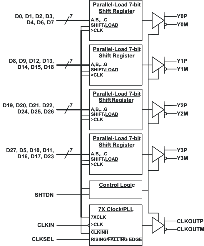
SN75LVDS83BDGG 电路图
SN75LVDS83BDGG 相关产品
- 29F52SC
- AD8016ARBZ
- AD8016ARBZ-REEL
- AD8016AREZ
- AD8016AREZ-REEL
- AD8016AREZ-REEL7
- AD8018ARUZ-REEL
- AD8018ARZ-REEL7
- AD807A-155BRZRL
- AD807A-155BRZRL7
- AD8128ACPZ-R7
- AD8145WYCPZ-R7
- AD8145YCPZ-R7
- AD8392AACPZ-RL
- AD8392AAREZ
- AD8392AAREZ-RL
- ADM1181AANZ
- ADM1385ARSZ-REEL
- ADM1385ARSZ-REEL7
- ADM1485ARMZ-REEL
- ADM1485ARMZ-REEL7
- ADM1485ARZ
- ADM1485JNZ
- ADM1486AR-REEL7
- ADM1486ARZ-REEL7
- ADM1490EBRMZ-REEL7
- ADM1490EBRZ
- ADM1490EBRZ-REEL7
- ADM202EARN-REEL
- ADM202EARNZ-REEL7