 搜索
搜索
 发布采购
发布采购
- 封装:56-TFSOP(0.240",6.10mm 宽)
- RoHS:无铅 / 符合限制有害物质指令(RoHS)规范要求
- 包装方式:Digi-Reel®
- 参考价格:$2.9664-$5.93
更新日期:2024-04-01 00:04:00
产品简介:FlatLink™ 接收器
查看详情- 封装:56-TFSOP(0.240",6.10mm 宽)
- RoHS:无铅 / 符合限制有害物质指令(RoHS)规范要求
- 包装方式:Digi-Reel®
- 参考价格:$2.9664-$5.93
SN75LVDS82DGGR 供应商
- 公司
- 型号
- 品牌
- 封装/批号
- 数量
- 地区
- 日期
- 说明
- 询价
-
TI
-
TSSOP56
22+ -
2685
-
上海市
-
-
-
原厂原装上海仓现货
-
TI/德州仪器
-
TSSOP56
21+ -
2000
-
杭州
-
-
-
只做原装现货,大量现货热卖
-
TI(德州仪器)
-
TSSOP-56
2022+ -
12000
-
上海市
-
-
-
原装可开发票
-
TI
-
TSSOP56
23+ -
5800
-
上海市
-
-
-
进口原装现货,杜绝假货。
-
TI
-
TSSOP56
23+ -
46000
-
合肥
-
-
-
科大讯飞战略投资企业,提供一站式配套服务
SN75LVDS82DGGR 中文资料属性参数
- 标准包装:1
- 类别:集成电路 (IC)
- 家庭:接口 - 驱动器,接收器,收发器
- 系列:FlatLink™
- 类型:接收器
- 驱动器/接收器数:0/5
- 规程:LVDS
- 电源电压:3 V ~ 3.6 V
- 安装类型:表面贴装
- 封装/外壳:56-TFSOP(0.240",6.10mm 宽)
- 供应商设备封装:56-TSSOP
- 包装:®
- 其它名称:296-6666-6
产品特性
- 4:28 Data Channel Expansion at up to 1904 Mbps Throughput
- Suited for SVGA, XGA, or SXGA Display Data Transmission From Controller to Display With Very Low EMI
- Four Data Channels and Clock Low-Voltage Differential Channels In and 28 Data and Clock Low-Voltage TTL Channels Out
- Operates From a Single 3.3-V Supply With 250 mW (Typical)
- 5-V Tolerant SHTDN Input
- Falling Clock-Edge-Triggered Outputs
- Packaged in Thin Shrink Small-Outline Package (TSSOP) With 20-Mil Terminal Pitch
- Consumes Less Than 1 mW When Disabled
- Pixel Clock Frequency Range of 31 MHz to 68 MHz
- No External Components Required for PLL
- Inputs Meet or Exceed the Requirements of ANSI EIA/TIA-644 Standard
产品概述
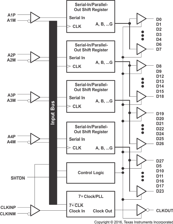
The SN75LVDS82 FlatLink™ receiver contains four
serial-in, 7-bit parallel-out shift registers, a 7× clock synthesizer, and five low-voltage
differential signaling (LVDS) line receivers in a single integrated circuit. These functions allow receipt of synchronous data from a compatible transmitter, such as
the SN75LVDS83B, over five balanced-pair conductors, and expansion to 28 bits of single-ended
low-voltage TTL (LVTTL) synchronous data at a lower transfer rate. The SN75LVDS82 can also be used
with the SN75LVDS84 for 21-bit transfers.When receiving, the high-speed LVDS data is received and loaded into registers at the
rate of seven times (7×) the LVDS input clock (CLKIN). The data is then unloaded to a 28-bit-wide
LVTTL parallel bus at the CLKIN rate. A phase-locked loop (PLL) clock synthesizer circuit generates
a 7× clock for internal clocking and an output clock for the expanded data. The SN75LVDS82 presents
valid data on the falling edge of the output clock (CLKOUT).The SN75LVDS82 requires only five line-termination resistors for the differential inputs
and little or no control. The data bus appears the same at the input to the transmitter and output
of the receiver with the data transmission transparent to the user.The only possible user intervention is the use of the shutdown/clear
(SHTDN) active-low input to inhibit the clock and shut off the LVDS
receivers for lower power consumption. A low-level on SHTDN clears all
internal registers to a low level and places the TTL outputs in a high-impedance state.The SN75LVDS82 is characterized for operation over ambient air temperatures of 0°C to
70°C.
SN75LVDS82DGGR 数据手册
| 数据手册 | 说明 | 数量 | 操作 |
|---|---|---|---|
 SN75LVDS82DGGR SN75LVDS82DGGR
|
FlatLink(TM) Receiver 56-TSSOP 0 to 70 |
15页,159K | 查看 |
|
SN75LVDS82DGGRG4
|
FlatLink(TM) Receiver 56-TSSOP 0 to 70 |
15页,159K | 查看 |
SN75LVDS82DGGR 电路图
SN75LVDS82DGGR 电路图
SN75LVDS82DGGR 相关产品
- 29F52SC
- AD8016ARBZ
- AD8016ARBZ-REEL
- AD8016AREZ
- AD8016AREZ-REEL
- AD8016AREZ-REEL7
- AD8018ARUZ-REEL
- AD8018ARZ-REEL7
- AD807A-155BRZRL
- AD807A-155BRZRL7
- AD8128ACPZ-R7
- AD8145WYCPZ-R7
- AD8145YCPZ-R7
- AD8392AACPZ-RL
- AD8392AAREZ
- AD8392AAREZ-RL
- ADM1181AANZ
- ADM1385ARSZ-REEL
- ADM1385ARSZ-REEL7
- ADM1485ARMZ-REEL
- ADM1485ARMZ-REEL7
- ADM1485ARZ
- ADM1485JNZ
- ADM1486AR-REEL7
- ADM1486ARZ-REEL7
- ADM1490EBRMZ-REEL7
- ADM1490EBRZ
- ADM1490EBRZ-REEL7
- ADM202EARN-REEL
- ADM202EARNZ-REEL7