 搜索
搜索
 发布采购
发布采购
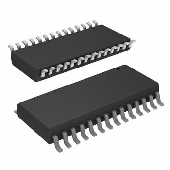
- 封装:28-SOIC(0.295",7.50mm 宽)
- RoHS:无铅 / 符合限制有害物质指令(RoHS)规范要求
- 包装方式:带卷 (TR)
- 参考价格:$2.03
更新日期:2024-04-01 00:04:00
产品简介:低功耗 LinBiCMOS 多路驱动器和接收器
查看详情- 封装:28-SOIC(0.295",7.50mm 宽)
- RoHS:无铅 / 符合限制有害物质指令(RoHS)规范要求
- 包装方式:带卷 (TR)
- 参考价格:$2.03
SN75LBC241DWR 供应商
- 公司
- 型号
- 品牌
- 封装/批号
- 数量
- 地区
- 日期
- 说明
- 询价
-
TI
-
原厂原装
22+ -
3288
-
上海市
-
-
-
一级代理原装
SN75LBC241DWR 中文资料属性参数
- 标准包装:1,000
- 类别:集成电路 (IC)
- 家庭:接口 - 驱动器,接收器,收发器
- 系列:-
- 类型:收发器
- 驱动器/接收器数:4/5
- 规程:RS232
- 电源电压:4.5 V ~ 5.5 V
- 安装类型:表面贴装
- 封装/外壳:28-SOIC(0.295",7.50mm 宽)
- 供应商设备封装:28-SOIC
- 包装:带卷 (TR)
产品特性
- Operates With Single 5-V Power Supply
- Meets or Exceeds the Requirements of TIA/EIA-232-F and ITU Recommendation V.28
- Improved Performance Replacement for MAX241
- Operates at Data Rates up to 100 kbit/s Over a 3-m Cable
- Low-Power Shutdown Mode... 1 uA Typ
- LinBiCMOSTM Process Technology
- Four Drivers and Five Receivers
- ±30-V Input Levels
- 3-State TTL/CMOS Receiver Outputs
- ±9-V Output Swing With a 5-V Supply
- Applications TIA/EIA-232-F Interface Battery-Powered Systems Terminals Modems Computers
- TIA/EIA-232-F Interface
- Battery-Powered Systems
- Terminals
- Modems
- Computers
- Packaged in Plastic Small-Outline Package
产品概述
The SN75LBC241 is a low-power LinBiCMOSTM line-interface device containing four independent drivers and five receivers. It is designed as a plug-in replacement for the Maxim MAX241. The SN75LBC241 provides a capacitive-charge-pump voltage generator to produce RS-232 voltage levels from a 5-V supply. The charge-pump oscillator frequency is 20 kHz. Each receiver converts RS-232 inputs to 5-V TTL/CMOS levels. The receivers have a typical threshold of 1.2 V and a typical hysteresis of 0.5 V and can accept ±30-V inputs. Each driver converts TTL/CMOS input levels into RS-232 levels.
The SN75LBC241 includes a receiver, a 3-state control line, and a low-power shutdown control line. When the EN\ line is high, receiver outputs are placed in the high-impedance state. When EN\ is low, normal operation is enabled.
The shutdown mode reduces power dissipation to less than 5 uW, typically. In this mode, receiver outputs have high impedance, driver outputs are turned off, and the charge-pump circuit is turned off. When SHUTDOWN is high, the shutdown mode is enabled. When SHUTDOWN is low, normal operation is enabled.
This device has been designed to conform to TIA/EIA-232-F and ITU Recommendation V.28.
The SN75LBC241 has been designed using LinBiCMOS technology and cells contained in the Texas Instruments LinASICTM library. Use of LinBiCMOS circuitry increases latch-up immunity in this device over an all-CMOS design.
The SN75LBC241 is characterized for operation from 0°C to 70°C.
SN75LBC241DWR 数据手册
| 数据手册 | 说明 | 数量 | 操作 |
|---|---|---|---|
 SN75LBC241DWRE4 SN75LBC241DWRE4
|
Low-Power LinBiCMOS Multiple Drivers And Receivers 28-SOIC 0 to 70 |
12页,386K | 查看 |
SN75LBC241DWR 相关产品
- 29F52SC
- AD8016ARBZ
- AD8016ARBZ-REEL
- AD8016AREZ
- AD8016AREZ-REEL
- AD8016AREZ-REEL7
- AD8018ARUZ-REEL
- AD8018ARZ-REEL7
- AD807A-155BRZRL
- AD807A-155BRZRL7
- AD8128ACPZ-R7
- AD8145WYCPZ-R7
- AD8145YCPZ-R7
- AD8392AACPZ-RL
- AD8392AAREZ
- AD8392AAREZ-RL
- ADM1181AANZ
- ADM1385ARSZ-REEL
- ADM1385ARSZ-REEL7
- ADM1485ARMZ-REEL
- ADM1485ARMZ-REEL7
- ADM1485ARZ
- ADM1485JNZ
- ADM1486AR-REEL7
- ADM1486ARZ-REEL7
- ADM1490EBRMZ-REEL7
- ADM1490EBRZ
- ADM1490EBRZ-REEL7
- ADM202EARN-REEL
- ADM202EARNZ-REEL7