 搜索
搜索
 发布采购
发布采购
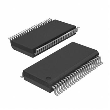
- 封装:48-BSSOP(0.295",7.50mm 宽)
- RoHS:无铅 / 符合限制有害物质指令(RoHS)规范要求
- 包装方式:管件
- 参考价格:$1.6
更新日期:2024-04-01 00:04:00
产品简介:具有 TTL 兼容型 CMOS 输入和三态输出的 16 通道、2.7V 至 3.6V 反相器
查看详情- 封装:48-BSSOP(0.295",7.50mm 宽)
- RoHS:无铅 / 符合限制有害物质指令(RoHS)规范要求
- 包装方式:管件
- 参考价格:$1.6
SN74LVT16240DL 供应商
- 公司
- 型号
- 品牌
- 封装/批号
- 数量
- 地区
- 日期
- 说明
- 询价
-
TI
-
原厂原装
22+ -
3288
-
上海市
-
-
-
一级代理原装
-
TI(德州仪器)
-
SSOP-48
2022+ -
12000
-
上海市
-
-
-
原装可开发票
SN74LVT16240DL 中文资料属性参数
- 标准包装:25
- 类别:集成电路 (IC)
- 家庭:逻辑 - 栅极和逆变器
- 系列:74LVT
- 逻辑类型:逆变器,缓冲器
- 电路数:4
- 输入数:4
- 特点:三态
- 电源电压:2.7 V ~ 3.6 V
- 电流 - 静态(最大值):5mA
- 输出电流高,低:32mA,64mA
- 逻辑电平 - 低:0.8V
- 逻辑电平 - 高:2V
- 额定电压和最大 CL 时的最大传播延迟:3.5ns @ 3.3V,50pF
- 工作温度:-40°C ~ 85°C
- 安装类型:表面贴装
- 供应商设备封装:48-SSOP
- 封装/外壳:48-BSSOP(0.295",7.50mm 宽)
- 包装:管件
产品特性
- Members of the Texas Instruments Widebus™ Family
- State-of-the-Art Advanced BiCMOS Technology (ABT) Design for 3.3-V Operation and Low Static-Power Dissipation
- Support Mixed-Mode Signal Operation (5-V Input and Output Voltages With 3.3-V VCC)
- Support Unregulated Battery Operation Down to 2.7 V
- Typical VOLP (Output Ground Bounce) <0.8 V at VCC = 3.3 V, TA = 25°C
- Ioff and Power-Up 3-State Support Hot Insertion
- Distributed VCC and GND Pins Minimize High-Speed Switching Noise
- Flow-Through Architecture Optimizes PCB Layout
- Latch-Up Performance Exceeds 100 mA Per JESD 78, Class II
- ESD Protection Exceeds JESD 222000-V Human-Body Model (A114-A)200-V Machine Model (A115-A)1000-V Charged-Device Model (C101)
- 2000-V Human-Body Model (A114-A)
- 200-V Machine Model (A115-A)
- 1000-V Charged-Device Model (C101)
- Package Options Include Plastic Shrink Small-Outline (DL) and Thin Shrink Small-Outline (DGG) Packages and 380-mil Fine-Pitch Ceramic Flat (WD) Package Using 25-mil Center-to-Center Spacings
产品概述
The 'LVT16240 devices are 16-bit buffers and line drivers designed specifically for low-voltage (3.3-V) VCC operation, but with the capability to provide a TTL interface to a 5-V system environment.These devices are designed specifically to improve both the performance and density of 3-state memory address drivers, clock drivers, and bus-oriented receivers and transmitters.The devices can be used as four 4-bit buffers, two 8-bit buffers, or one 16-bit buffer. The devices provide inverting outputs and symmetrical active-low output-enable (OE) inputs.When VCC is between 0 and 1.5 V, the devices are in the high-impedance state during power up or power down. However, to ensure the high-impedance state above 1.5 V, OE should be tied to VCC through a pullup resistor; the minimum value of the resistor is determined by the current-sinking capability of the driver.These devices are fully specified for hot-insertion applications using Ioff and power-up 3-state. The Ioff circuitry disables the outputs, preventing damaging current backflow through the devices when they are powered down. The power-up 3-state circuitry places the outputs in the high-impedance state during power up and power down, which prevents driver conflict.The SN54LVT16240 is characterized for operation over the full military temperature range of -55°C to 125°C. The SN74LVT16240 is characterized for operation from -40°C to 85°C.
SN74LVT16240DL 数据手册
| 数据手册 | 说明 | 数量 | 操作 |
|---|---|---|---|
 SN74LVT16240DLR SN74LVT16240DLR
|
Buffer, Inverting 4 Element 4 Bit per Element Push-Pull Output 48-SSOP |
13页,317K | 查看 |
SN74LVT16240DL 相关产品
- 1A1G04QDBVRG4Q1
- 1P1G08MDBVREPG4
- 1P1G14MDBVREPG4
- 74ABT240CSCX
- 74ABT240DB,118
- 74AC00SJX
- 74AC04SJX
- 74AC11000DR
- 74AC11000N
- 74AC11004DWR
- 74AC11004N
- 74AC11008D
- 74AC11008N
- 74AC11008PWR
- 74AC11032D
- 74AC11032DBR
- 74AC11032N
- 74AC11032NSR
- 74AC11086D
- 74AC11086N
- 74AC11240DBR
- 74AC11240DW
- 74AC11240PW
- 74AC11SJX
- 74AC14SJ
- 74AC20PC
- 74AC240MTCX
- 74AC240MTR
- 74AC240SC
- 74AC32SJ