 搜索
搜索
 发布采购
发布采购
- 封装:8-XFBGA,DSBGA
- RoHS:无铅 / 符合限制有害物质指令(RoHS)规范要求
- 包装方式:Digi-Reel®
- 参考价格:$0.252-$0.7
更新日期:2024-04-01 00:04:00

产品简介:2 通道、2 输入、1.65V 至 5.5V、32mA 驱动强度与门
查看详情- 封装:8-XFBGA,DSBGA
- RoHS:无铅 / 符合限制有害物质指令(RoHS)规范要求
- 包装方式:Digi-Reel®
- 参考价格:$0.252-$0.7
SN74LVC2G08YZPR 供应商
- 公司
- 型号
- 品牌
- 封装/批号
- 数量
- 地区
- 日期
- 说明
- 询价
-
TI
-
原厂原装
22+ -
3288
-
上海市
-
-
-
一级代理原装
-
TI(德州仪器)
-
DSBGA-8
2022+ -
334
-
上海市
-
-
-
原装可开发票
-
TexasInst
-
BGA
新批号 -
887000
-
上海市
-
-
-
原厂发货进口原装微信同步QQ893727827
-
TI
-
-
2021+ -
28000
-
苏州
-
-
-
TI
-
TSSOP
23+ -
46000
-
合肥
-
-
-
科大讯飞战略投资企业,提供一站式配套服务
SN74LVC2G08YZPR 中文资料属性参数
- 标准包装:1
- 类别:集成电路 (IC)
- 家庭:逻辑 - 栅极和逆变器
- 系列:74LVC
- 逻辑类型:与门
- 电路数:2
- 输入数:2
- 特点:-
- 电源电压:1.65 V ~ 5.5 V
- 电流 - 静态(最大值):10µA
- 输出电流高,低:32mA,32mA
- 逻辑电平 - 低:0.7 V ~ 0.8 V
- 逻辑电平 - 高:1.7 V ~ 2 V
- 额定电压和最大 CL 时的最大传播延迟:3.8ns @ 5V,50pF
- 工作温度:-40°C ~ 85°C
- 安装类型:表面贴装
- 供应商设备封装:8-DSBGA,8-WCSP(1.9x0.9)
- 封装/外壳:8-XFBGA,DSBGA
- 包装:®
- 其它名称:296-14371-6
产品特性
- Available in the Texas Instruments NanoStar™ and NanoFree™ Package
- Supports 5-V VCC Operation
- Inputs Accept Voltages to 5.5 V
- Max tpd of 4.7 ns at 3.3 V
- Low Power Consumption, 10-µA Maximum ICC
- ±24-mA Output Drive at 3.3 V
- Typical VOLP (Output Ground Bounce) <0.8 V at VCC = 3.3 V, TA = 25°C
- Typical VOHV (Output VOH Undershoot) >2 V at VCC = 3.3 V, TA = 25°C
- Ioff Supports Live Insertion, Partial-Power-Down Mode, and Back-Drive Protection
- Can Be Used as a Down Translator to Translate Inputs From a Maximum of 5.5 V Down to the VCC Level
- Latch-Up Performance Exceeds 100 mA Per JESD 78, Class II
- ESD Protection Exceeds JESD 22 2000-V Human Body Model (A114-A) 1000-V Charged-Device Model (C101)
- 2000-V Human Body Model (A114-A)
- 1000-V Charged-Device Model (C101)
产品概述
This dual 2-input positive-AND gate is designed for 1.65-V to 5.5-V
VCC operation.The SN74LVC2G08 device performs the Boolean function A × B or Y = A\ + B\ in positive logic.NanoFree package technology is a major breakthrough in IC packaging concepts, using the
die as the package.This device is fully specified for partial-power-down applications using
Ioff. The Ioff circuitry disables the outputs,
preventing damaging current backflow through the device when it is powered down.
SN74LVC2G08YZPR 数据手册
| 数据手册 | 说明 | 数量 | 操作 |
|---|---|---|---|
 SN74LVC2G08YZPR SN74LVC2G08YZPR
|
DUAL 2 INPUT POSITIVE AND GATE |
12 Pages页,320K | 查看 |
SN74LVC2G08YZPR 电路图
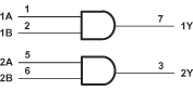
SN74LVC2G08YZPR 电路图
SN74LVC2G08YZPR 相关产品
- 1A1G04QDBVRG4Q1
- 1P1G08MDBVREPG4
- 1P1G14MDBVREPG4
- 74ABT240CSCX
- 74ABT240DB,118
- 74AC00SJX
- 74AC04SJX
- 74AC11000DR
- 74AC11000N
- 74AC11004DWR
- 74AC11004N
- 74AC11008D
- 74AC11008N
- 74AC11008PWR
- 74AC11032D
- 74AC11032DBR
- 74AC11032N
- 74AC11032NSR
- 74AC11086D
- 74AC11086N
- 74AC11240DBR
- 74AC11240DW
- 74AC11240PW
- 74AC11SJX
- 74AC14SJ
- 74AC20PC
- 74AC240MTCX
- 74AC240MTR
- 74AC240SC
- 74AC32SJ