 搜索
搜索
 发布采购
发布采购
更新日期:2024-04-01 00:04:00

产品简介:具有漏极开路输出的单路 2 输入、1.65V 至 5.5V 与非门
查看详情SN74LVC1G38DPWR 供应商
- 公司
- 型号
- 品牌
- 封装/批号
- 数量
- 地区
- 日期
- 说明
- 询价
-
TI
-
原厂原装
22+ -
3288
-
上海市
-
-
-
一级代理原装
-
TI(德州仪器)
-
X2SON-5
2022+ -
12000
-
上海市
-
-
-
原装可开发票
SN74LVC1G38DPWR 中文资料属性参数
- 现有数量:641现货9,000Factory
- 价格:1 : ¥3.10000剪切带(CT)3,000 : ¥1.01004卷带(TR)
- 系列:74LVC
- 包装:卷带(TR)剪切带(CT)? 得捷定制卷带
- 产品状态:在售
- 逻辑类型:与非门
- 电路数:1
- 输入数:2
- 特性:开路漏极
- 电压 - 供电:1.65V ~ 5.5V
- 电流 - 静态(最大值):10 μA
- 电流 - 输出高、低:-,32mA
- 逻辑电平 - 低:0.7V ~ 0.8V
- 逻辑电平 - 高:1.2V ~ 2V
- 不同 V、最大 CL 时最大传播延迟:4.4ns @ 5V,50pF
- 工作温度:-40°C ~ 85°C
- 安装类型:表面贴装型
- 供应商器件封装:5-X2SON(0.8x0.8)
- 封装/外壳:4-XFDFN 裸露焊盘
产品特性
- Latch-up performance exceeds 100 mA Per JESD 78, Class II
- ESD protection exceeds JESD 22 2000-V Human-body model (A114-A) 200-V Machine model (A115-A) 1000-V Charged-device model (C101)
- 2000-V Human-body model (A114-A)
- 200-V Machine model (A115-A)
- 1000-V Charged-device model (C101)
- Available in the Texas Instruments NanoStar™ and NanoFree™ Packages
- Supports 5-V VCC operation
- Inputs accept voltages to 5.5 V
- Supports down translation to VCC
- Maximum tpd of 4.5 ns at 3.3 V
- Low power consumption, 10-µA maximum ICC
- ±24-mA Output drive at 3.3 V
- Ioff Supports partial-power-down mode and back-drive protection
产品概述
The SN74LVC1G38 device is designed for 1.65-V to 5.5-V VCC
operation.This device is a single two-input NAND buffer gate with open-drain output. It performs
the Boolean function Y = A × B or Y = A +
B in positive logic.This device is fully specified for partial-power-down applications using
Ioff. The Ioff circuitry disables the outputs when
the device is powered down. This inhibits current backflow into the device which prevents damage to
the device.NanoStar™ and NanoFree™ package technology is a major breakthrough in IC packaging
concepts, using the die as the package.
SN74LVC1G38DPWR 电路图
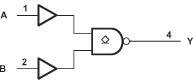
SN74LVC1G38DPWR 电路图
SN74LVC1G38DPWR 相关产品
- 1P1G125QDRYRQ1
- 1P1G126QDRYRQ1
- 1P2GU04QDRYRQ1
- 2N7001TDCKR
- 2N7001TDPWR
- 54FCT245TDB
- 5962-8762401CA
- 5962-8766301MRA
- 5962-8768001EA
- 7202LA50JG
- 7203L20TDB
- 7204L35J
- 72805LB15PF
- 7280L20PA
- 72V201L15PFGI
- 72V211L10PFG
- 72V245L10PFG
- 72V3640L10PF
- 72V3660L7-5PFI
- 72V70210DAG
- 72V70840DAG
- 72V73273BBG
- 74AHC05S14-13
- 74AHC05T14-13
- 74AHC1G126MDCKTEP
- 74AHC32S14-13
- 74AHC594S16-13
- 74AHC594T16-13
- 74AHCT08PW-Q100J
- 74AHCT125S14-13