 搜索
搜索
 发布采购
发布采购
更新日期:2024-04-01 00:04:00

产品简介:具有施密特触发输入的单路 0.8V 至 3.6V 低功耗反相器
查看详情SN74AUP1G14DPWR 供应商
- 公司
- 型号
- 品牌
- 封装/批号
- 数量
- 地区
- 日期
- 说明
- 询价
-
TI
-
原厂原装
22+ -
3288
-
上海市
-
-
-
一级代理原装
-
TI(德州仪器)
-
X2SON-5
2022+ -
12000
-
上海市
-
-
-
原装可开发票
SN74AUP1G14DPWR 中文资料属性参数
- 现有数量:545现货9,000Factory
- 价格:1 : ¥4.05000剪切带(CT)3,000 : ¥1.29385卷带(TR)
- 系列:74AUP
- 包装:卷带(TR)剪切带(CT)? 得捷定制卷带
- 产品状态:在售
- 逻辑类型:反相器
- 电路数:1
- 输入数:1
- 特性:施密特触发器
- 电压 - 供电:0.8V ~ 3.6V
- 电流 - 静态(最大值):500 nA
- 电流 - 输出高、低:4mA,4mA
- 逻辑电平 - 低:0.1V ~ 0.8V
- 逻辑电平 - 高:0.6V ~ 2.29V
- 不同 V、最大 CL 时最大传播延迟:6.2ns @ 3.3V,30pF
- 工作温度:-40°C ~ 85°C
- 安装类型:表面贴装型
- 供应商器件封装:5-X2SON(0.8x0.8)
- 封装/外壳:4-XFDFN 裸露焊盘
产品特性
- Latch-Up Performance Exceeds 100 mA Per JESD 78, Class II
- ESD Performance Tested Per JESD 222000-V Human-Body Model (A114-B, Class II)1000-V Charged-Device Model (C101)
- 2000-V Human-Body Model (A114-B, Class II)
- 1000-V Charged-Device Model (C101)
- Low Static-Power Consumption (ICC = 0.9 µA Maximum)
- Low Dynamic-Power Consumption (Cpd = 4.4 pF Typical at 3.3 V)
- Low Input Capacitance (CI = 1.5 pF Typical)
- Low Noise – Overshoot and Undershoot <10% of VCC
- Ioff Supports Partial-Power-Down Mode Operation
- Includes Schmitt-Trigger Inputs
- Wide Operating VCC Range of 0.8 V to 3.6 V
- Optimized for 3.3-V Operation
- 3.6-V I/O Tolerant to Support Mixed-Mode Signal Operation
- tpd = 4.9 ns Maximum at 3.3 V
产品概述
The AUP family is TI’s premier solution to the industry’s low power needs in
battery-powered portable applications. This family assures a very low static and dynamic power
consumption across the entire VCC range of 0.8 V to 3.6 V, resulting in an
increased battery life. This product also maintains excellent signal integrity (see
AUP – The Lowest-Power Family and
Excellent Signal Integrity).This device functions as an independent gate with Schmitt-trigger inputs, which allows
for slow input transition and better switching-noise immunity at the input. This device is fully specified for partial-power-down applications using
Ioff. The Ioff circuitry disables the outputs when
the device is powered down. This inhibits current backflow into the device which prevents damage to
the device.
SN74AUP1G14DPWR 电路图
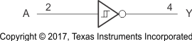
SN74AUP1G14DPWR 电路图
SN74AUP1G14DPWR 相关产品
- 1P1G125QDRYRQ1
- 1P1G126QDRYRQ1
- 1P2GU04QDRYRQ1
- 2N7001TDCKR
- 2N7001TDPWR
- 54FCT245TDB
- 5962-8762401CA
- 5962-8766301MRA
- 5962-8768001EA
- 7202LA50JG
- 7203L20TDB
- 7204L35J
- 72805LB15PF
- 7280L20PA
- 72V201L15PFGI
- 72V211L10PFG
- 72V245L10PFG
- 72V3640L10PF
- 72V3660L7-5PFI
- 72V70210DAG
- 72V70840DAG
- 72V73273BBG
- 74AHC05S14-13
- 74AHC05T14-13
- 74AHC1G126MDCKTEP
- 74AHC32S14-13
- 74AHC594S16-13
- 74AHC594T16-13
- 74AHCT08PW-Q100J
- 74AHCT125S14-13