 搜索
搜索
 发布采购
发布采购
更新日期:2024-04-01 00:04:00

产品简介:SN74AHC8541
查看详情SN74AHC8541N 供应商
- 公司
- 型号
- 品牌
- 封装/批号
- 数量
- 地区
- 日期
- 说明
- 询价
-
TI
-
原厂原装
22+ -
3288
-
上海市
-
-
-
一级代理原装
-
TI(德州仪器)
-
PDIP-20
2022+ -
12000
-
上海市
-
-
-
原装可开发票
SN74AHC8541N 中文资料属性参数
- 现有数量:857现货9,460Factory
- 价格:1 : ¥12.00000管件
- 系列:74AHC
- 包装:管件
- 产品状态:在售
- 逻辑类型:缓冲器,反向,非反向
- 元件数:1
- 每个元件位数:8
- 输入类型:施密特触发器
- 输出类型:三态
- 电流 - 输出高、低:12mA,12mA
- 电压 - 供电:2V ~ 5.5V
- 工作温度:-40°C ~ 85°C(TA)
- 安装类型:通孔
- 封装/外壳:20-DIP(0.300",7.62mm)
- 供应商器件封装:20-PDIP
产品特性
- Operating Range of 2 V to 5.5 V VCC
- 8-Bit Inverting/Non-Inverting Outputs
- 20-Pin Thin Shrink Small-Outline Package [TSSOP (PW)] and 20-Pin Plastic Dual-In-Line Package [PDIP (N)]
产品概述
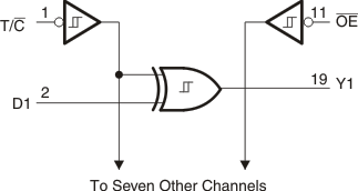
The SN74AHC8541 8-bit inverting/non-inverting buffers are ideal for driving bus lines or
buffer memory address registers. These devices feature inputs and outputs on opposite sides of the
package to facilitate printed circuit board layout.All outputs are in the high-impedance state (disabled) when the output-enable
(OE) input is high. When OE is low, the respective
gate passes the data from the D input to its Y output.The T/C input selects inverting or non-inverting data transfer.
When the T/C input is high, it provides non-inverting buffers. When the
T/C input is low, it provides inverting buffers when they are not in the
high-impedance state.To ensure the high-impedance state during power up or power down,
OE should be tied to VCC through a pullup resistor;
the minimum value of the resistor is determined by the current-sinking capability of the
driver.
SN74AHC8541N 电路图
SN74AHC8541N 电路图
SN74AHC8541N 相关产品
- 1P1G125QDRYRQ1
- 1P1G126QDRYRQ1
- 1P2GU04QDRYRQ1
- 2N7001TDCKR
- 2N7001TDPWR
- 54FCT245TDB
- 5962-8762401CA
- 5962-8766301MRA
- 5962-8768001EA
- 7202LA50JG
- 7203L20TDB
- 7204L35J
- 72805LB15PF
- 7280L20PA
- 72V201L15PFGI
- 72V211L10PFG
- 72V245L10PFG
- 72V3640L10PF
- 72V3660L7-5PFI
- 72V70210DAG
- 72V70840DAG
- 72V73273BBG
- 74AHC05S14-13
- 74AHC05T14-13
- 74AHC1G126MDCKTEP
- 74AHC32S14-13
- 74AHC594S16-13
- 74AHC594T16-13
- 74AHCT08PW-Q100J
- 74AHCT125S14-13