 搜索
搜索
 发布采购
发布采购
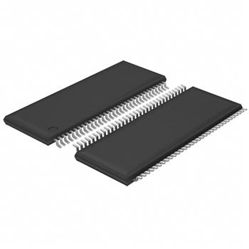
- 封装:64-TFSOP (0.240",6.10mm 宽)
- RoHS:无铅 / 符合限制有害物质指令(RoHS)规范要求
- 包装方式:带卷 (TR)
- 参考价格:$3.9
更新日期:2024-04-01 00:04:00
产品简介:8 通道半双工 M-LVDS 收发器
查看详情- 封装:64-TFSOP (0.240",6.10mm 宽)
- RoHS:无铅 / 符合限制有害物质指令(RoHS)规范要求
- 包装方式:带卷 (TR)
- 参考价格:$3.9
SN65MLVD082DGGR 供应商
- 公司
- 型号
- 品牌
- 封装/批号
- 数量
- 地区
- 日期
- 说明
- 询价
-
TI
-
原厂原装
22+ -
3288
-
上海市
-
-
-
一级代理原装
-
TI/德州仪器
-
TSSOP64
21+ -
10000
-
杭州
-
-
-
只做原装现货,大量现货热卖
-
TI(德州仪器)
-
TSSOP-64
2022+ -
12000
-
上海市
-
-
-
原装可开发票
SN65MLVD082DGGR 中文资料属性参数
- 标准包装:2,000
- 类别:集成电路 (IC)
- 家庭:接口 - 驱动器,接收器,收发器
- 系列:-
- 类型:收发器
- 驱动器/接收器数:8/8
- 规程:LVDS,多点
- 电源电压:3 V ~ 3.6 V
- 安装类型:表面贴装
- 封装/外壳:64-TFSOP (0.240",6.10mm 宽)
- 供应商设备封装:64-TSSOP
- 包装:带卷 (TR)
产品特性
- Low-Voltage Differential 30- Line Drivers and Receivers for Signaling Rates(1) Up to 250 Mbps; Clock Frequencies Up to 125 MHz
- Meets or Exceeds the M-LVDS Standard TIA/EIA-899 for Multipoint Data Interchange
- Controlled Driver Output Voltage Transition Times for Improved Signal Quality
- –1 V to 3.4 V Common-Mode Voltage Range Allows Data Transfer With 2 V of Ground Noise
- Bus Pins High Impedance When Driver Disabled or VCC ≤ 1.5 V
- Independent Enables for each Driver
- Bus Pin ESD Protection Exceeds 8 kV
- Packaged in 64-Pin TSSOP (DGG)
- M-LVDS Bus Power Up/Down Glitch Free
- APPLICATIONS Parallel Multipoint Data and Clock Transmission Via Backplanes and Cables Low-Power High-Speed Short-Reach Alternative to TIA/EIA-485 Cellular Base Stations Central-Office Switches Network Switches and Routers
- Parallel Multipoint Data and Clock Transmission Via Backplanes and Cables
- Low-Power High-Speed Short-Reach Alternative to TIA/EIA-485
- Cellular Base Stations
- Central-Office Switches
- Network Switches and Routers
产品概述
The SN65MLVD080 and SN65MLVD082 provide eight half-duplex transceivers for transmitting and receiving Multipoint-Low-Voltage Differential Signals in full compliance with the TIA/EIA-899 (M-LVDS) standard, which are optimized to operate at signaling rates up to 250 Mbps. The driver outputs have been designed to support multipoint buses presenting loads as low as 30- and incorporates controlled transition times to allow for stubs off of the backbone transmission line.The M-LVDS standard defines two types of receivers, designated as Type-1 and Type-2. Type-1 receivers (SN65MLVD080) have thresholds centered about zero with 25 mV of hysteresis to prevent output oscillations with loss of input; Type-2 receivers (SN65MLVD082) implement a failsafe by using an offset threshold. In addition, the driver rise and fall times are between 1 and 1.5 ns, complying with the M-LVDS standard to provide operation at 250 Mbps while also accommodating stubs on the bus. Receiver outputs are slew rate controlled to reduce EMI and crosstalk effects associated with large current surges. The M-LVDS standard allows for 32 nodes on the bus providing a high-speed replacement for RS-485 where lower common-mode can be tolerated or when higher signaling rates are needed.The driver logic inputs and the receiver logic outputs are on separate pins rather than tied together as in some transceiver designs. The drivers have separate enables (DE) and the receivers are enabled globally through (RE)\. This arrangement of separate logic inputs, logic outputs, and enable pins allows for a listen-while-talking operation. The devices are characterized for operation from –40°C to 85°C.
SN65MLVD082DGGR 数据手册
| 数据手册 | 说明 | 数量 | 操作 |
|---|---|---|---|
 SN65MLVD082DGGR SN65MLVD082DGGR
|
8-Channel Half-Duplex M-LVDS transceiver 64-TSSOP -40 to 85 |
28页,661K | 查看 |
|
SN65MLVD082DGGRG4
|
8-Channel Half-Duplex M-LVDS transceiver 64-TSSOP -40 to 85 |
28页,661K | 查看 |
SN65MLVD082DGGR 相关产品
- 29F52SC
- AD8016ARBZ
- AD8016ARBZ-REEL
- AD8016AREZ
- AD8016AREZ-REEL
- AD8016AREZ-REEL7
- AD8018ARUZ-REEL
- AD8018ARZ-REEL7
- AD807A-155BRZRL
- AD807A-155BRZRL7
- AD8128ACPZ-R7
- AD8145WYCPZ-R7
- AD8145YCPZ-R7
- AD8392AACPZ-RL
- AD8392AAREZ
- AD8392AAREZ-RL
- ADM1181AANZ
- ADM1385ARSZ-REEL
- ADM1385ARSZ-REEL7
- ADM1485ARMZ-REEL
- ADM1485ARMZ-REEL7
- ADM1485ARZ
- ADM1485JNZ
- ADM1486AR-REEL7
- ADM1486ARZ-REEL7
- ADM1490EBRMZ-REEL7
- ADM1490EBRZ
- ADM1490EBRZ-REEL7
- ADM202EARN-REEL
- ADM202EARNZ-REEL7