 搜索
搜索
 发布采购
发布采购
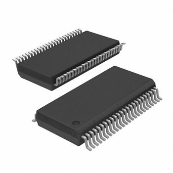
- 封装:48-TFSOP(0.240",6.10mm 宽)
- RoHS:无铅 / 符合限制有害物质指令(RoHS)规范要求
- 包装方式:管件
- 参考价格:$5.1075
更新日期:2024-04-01 00:04:00
产品简介:FlatLink 接收器
查看详情- 封装:48-TFSOP(0.240",6.10mm 宽)
- RoHS:无铅 / 符合限制有害物质指令(RoHS)规范要求
- 包装方式:管件
- 参考价格:$5.1075
SN65LVDS86AQDGG 供应商
- 公司
- 型号
- 品牌
- 封装/批号
- 数量
- 地区
- 日期
- 说明
- 询价
-
TI
-
原厂原装
22+ -
3288
-
上海市
-
-
-
一级代理原装
-
TI
-
-
2019+ -
5800
-
上海市
-
-
-
全新原装现货
-
TI(德州仪器)
-
TSSOP-48
2022+ -
5000
-
上海市
-
-
-
原装可开发票
-
TI
-
-
21+ -
100
-
上海市
-
-
-
原装现货,品质为先!请来电垂询!
SN65LVDS86AQDGG 中文资料属性参数
- 标准包装:40
- 类别:集成电路 (IC)
- 家庭:接口 - 专用
- 系列:65LVDS
- 应用:显示器
- 接口:串行
- 电源电压:3 V ~ 3.6 V
- 封装/外壳:48-TFSOP(0.240",6.10mm 宽)
- 供应商设备封装:48-TSSOP
- 包装:管件
- 安装类型:表面贴装
- 其它名称:296-9748-5
产品特性
- 3:21 Data Channel Expansion at up to 178.5 Mbytes/s Throughput
- Suited for SVGA, XGA, or SXGA Display Data Transmission From Controller to Display With Very Low EMI
- Three Data Channels and Clock Low-Voltage Differential Channels In and 21 Data and Clock Low-Voltage TTL Channels Out
- Operates From a Single 3.3-V Supply
- Tolerates 4-kV HBM ESD
- Packaged in Thin Shrink Small-Outline Package (TSSOP) With 20-Mil Terminal Pitch
- Consumes Less Than 1 mW When Disabled
- Wide Phase-Lock Input Frequency Range of 31 MHz to 68 MHz
- No External Components Required for PLL
- Inputs Meet or Exceed the Standard Requirements of ANSI EIA/TIA-644 Standard
- Improved Replacement for the DS90C364 and SN75LVDS86
- Improved Jitter Tolerance
- See SN65LVDS86A-Q1 Data Sheet for Information About the Automotive Qualified Version
产品概述
The SN65LVDS86A/SN75LVDS86A FlatLink. receiver contains three serial-in 7-bit parallel-out shift registers and four low-voltage differential signaling (LVDS) line receivers in a single integrated circuit. These functions allow receipt of synchronous data from a compatible transmitter, such as the SN75LVDS81, ’83, ’84, or ’85, over four balanced-pair conductors and expansion to 21 bits of single-ended low-voltage LVTTL synchronous data at a lower transfer rate.When receiving, the high-speed LVDS data is received and loaded into registers at seven times the LVDS input clock (CLKIN) rate. The data is then unloaded to a 21-bit-wide LVTTL parallel bus at the CLKIN rate. The ’LVDS86A presents valid data on the falling edge of the output clock (CLKOUT).The ’LVDS86A requires only four line-termination resistors for the differential inputs and little or no control. The data bus appears the same at the input to the transmitter and output of the receiver with the data transmission transparent to the user(s). The only user intervention is the possible use of the shutdown/clear (SHTDN) active-low input to inhibit the clock and shut off the LVDS receivers for lower power consumption. A low level on this signal clears all internal registers to a low level.The SN75LVDS86A is characterized for operation over ambient free-air temperatures of 0°C to 70°C. The SN65LVDS86A is characterized for operation over the full Automotive temperature range of –40°C to 125°C.
SN65LVDS86AQDGG 数据手册
| 数据手册 | 说明 | 数量 | 操作 |
|---|---|---|---|
 SN65LVDS86AQDGG SN65LVDS86AQDGG
|
Flatlink Receiver 48-TSSOP -40 to 125 |
0页,14K | 查看 |
|
SN65LVDS86AQDGGR
|
Flatlink Receiver 48-TSSOP -40 to 125 |
0页,14K | 查看 |
|
SN65LVDS86AQDGGR
|
Displays Interface 48-TSSOP |
18页,550K | 查看 |
|
SN65LVDS86AQDGGRQ1
|
Automotive Catalog FlatLink Receiver 48-TSSOP -40 to 125 |
15页,204K | 查看 |
|
SN65LVDS86AQDGGRQ1
|
Displays, Monitors, TV Interface 48-TSSOP |
17页,154K | 查看 |
SN65LVDS86AQDGG 相关产品
- AD6623ASZ
- AD6641BCPZ-500
- AD7569BNZ
- AD7569JRZ-REEL
- AD7569KNZ
- AD7669ARZ
- AD7669JNZ
- AD7669JPZ
- AD7669JRZ-REEL
- AD7868AR-REEL
- AD7868BNZ
- AD7868BR-REEL
- AD7868BRZ-REEL
- AD7869JNZ
- AD7869JRZ
- AD8156ABCZ
- AD8170ANZ
- AD8170ARZ-R7
- AD8170ARZ-RL
- AD8174AR
- AD8174ARZ-RL
- AD9882KSTZ-100
- AD9882KSTZ-140
- AD9883ABSTZ-RL110
- AD9887AKSZ-100
- AD9887AKSZ-140
- AD9888KSZ-100
- AD9980KSTZ-80
- AD9980KSTZ-95
- AD9985AKSTZ-140