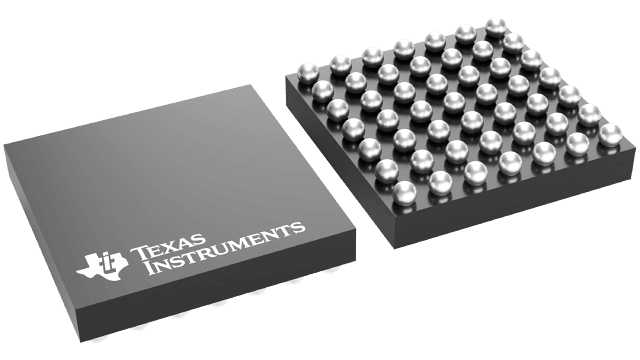
- 封装:49-UFBGA,DSBGA
- RoHS:无铅 / 符合限制有害物质指令(RoHS)规范要求
- 包装方式:Digi-Reel®
- 参考价格:$3.024-$6.05
更新日期:2024-04-01 00:04:00
产品简介:可编程 27 位显示屏串行接口变送器
查看详情- 封装:49-UFBGA,DSBGA
- RoHS:无铅 / 符合限制有害物质指令(RoHS)规范要求
- 包装方式:Digi-Reel®
- 参考价格:$3.024-$6.05
SN65LVDS311YFFR 供应商
- 公司
- 型号
- 品牌
- 封装/批号
- 数量
- 地区
- 日期
- 说明
- 询价
-
TI
-
原厂原装
22+ -
3288
-
上海市
-
-
-
一级代理原装
SN65LVDS311YFFR 中文资料属性参数
- 标准包装:1
- 类别:集成电路 (IC)
- 家庭:接口 - 专用
- 系列:65LVDS
- 应用:移动电话
- 接口:串行
- 电源电压:1.65 V ~ 1.95 V
- 封装/外壳:49-UFBGA,DSBGA
- 供应商设备封装:49-DSBGA(3x3)
- 包装:®
- 安装类型:表面贴装
- 其它名称:296-27594-6
产品特性
- 2.8 × 2.8mm package size
- 1.8V input signal swing
- 24-Bit RGB Data, 3 Control Bits, 1 Parity Bit and 2 Reserved Bits Transmitted over 1, 2 or 3 Differential Lines
- SubLVDS Differential Voltage Levels
- Three Operating Modes to Conserve Power Active-Mode QVGA 17.4mW (typ) Active-Mode VGA 28.8mW (typ) Shutdown Mode ≈ 0.5µA (typ) Standby Mode ≈ 0.5µA (typ)
- Active-Mode QVGA 17.4mW (typ)
- Active-Mode VGA 28.8mW (typ)
- Shutdown Mode ≈ 0.5µA (typ)
- Standby Mode ≈ 0.5µA (typ)
- ESD Rating > 3kV (HBM)
- Pixel Clock Range of 4MHz–65MHz
- Failsafe on all CMOS Inputs
- Typical Application: Cameras, Embedded Computers
产品概述
The SN65LVDS311 serializer transmits 27 parallel input data over 1, 2, or 3 serial output
links. The device pinout is optimized to interface with the OMAP3630 application processor. The
device loads a shift register with the 24 pixel bits and 3 control bits from the parallel CMOS
input interface. The data are latched into the device by the pixel clock, PCLK. In addition to the
27 bits, the device adds a parity bit and two reserved bits for a total number of 30 serial bits.
The parity bit allows a receiver to detect single-bit errors. Odd parity is implemented.The serial shift register is uploaded through 1, 2, or 3 serial outputs at 30, 15, or 10
times the pixel clock data rate. A copy of the pixel clock is output on an additional differential
output. The serial data and clock are transmitted via Sub Low-Voltage Differential Signaling
(SubLVDS) lines. The SN65LVDS311 supports three power modes (Shutdown, Standby and Active) to
conserve power.When transmitting, the PLL locks to the incoming pixel clock PCLK and generates an
internal high-speed clock at the line rate of the data lines. The parallel data is latched on the
rising edge of PCLK. The serialized data is presented on the serial outputs D0, D1, D2 with a
recreation of the Pixel clock PCLK generated from the internal high-speed clock and output on the
CLK output. If the input clock PCLK stops, the device enters a standby mode to conserve
power.Two Link-Select lines LS0 and LS1 control whether 1, 2 or 3 serial links are used. The
TXEN input may be used to put the SN65LVDS311 in a shutdown mode. The SN65LVDS311 enters an active
Standby mode if the input clock PCLK stops. This minimizes power consumption without the need for
controlling an external pin. The SN65LVDS311 is characterized for operation over ambient air
temperatures of -40°C to 85°C. All CMOS inputs offer failsafe to protect the input from damage
during power-up and to avoid current flow into the device inputs during power-up.
SN65LVDS311YFFR 相关产品
- AD6623ASZ
- AD6641BCPZ-500
- AD7569BNZ
- AD7569JRZ-REEL
- AD7569KNZ
- AD7669ARZ
- AD7669JNZ
- AD7669JPZ
- AD7669JRZ-REEL
- AD7868AR-REEL
- AD7868BNZ
- AD7868BR-REEL
- AD7868BRZ-REEL
- AD7869JNZ
- AD7869JRZ
- AD8156ABCZ
- AD8170ANZ
- AD8170ARZ-R7
- AD8170ARZ-RL
- AD8174AR
- AD8174ARZ-RL
- AD9882KSTZ-100
- AD9882KSTZ-140
- AD9883ABSTZ-RL110
- AD9887AKSZ-100
- AD9887AKSZ-140
- AD9888KSZ-100
- AD9980KSTZ-80
- AD9980KSTZ-95
- AD9985AKSTZ-140

 搜索
搜索
 发布采购
发布采购
